
Andrew Huang's Blog, page 9
February 27, 2023
Name that Ware, February 2023
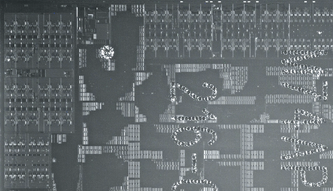
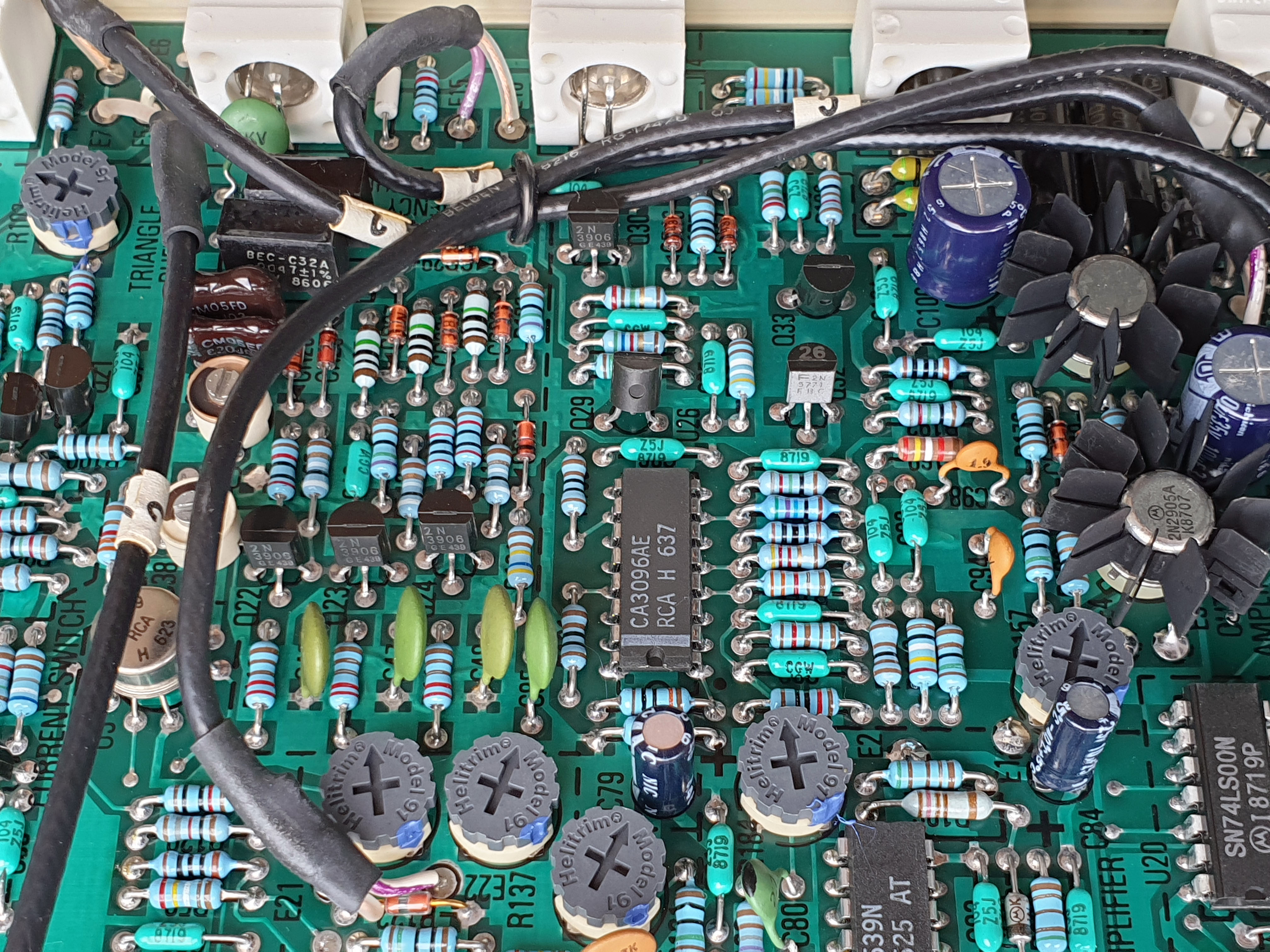
The Ware for February 2023 is shown below.

Just a small portion of the ware is shown here to make things a bit more challenging. If after a week it turns out to be too hard to guess based on the subtle details included in this image, I’ll add another image to this post with a bit more context.


Winner, Name that Ware January 2023
The Ware for January 2023 is a front-end readout board from the KASCADE muon detector. Thanks again to cpresser for contributing the ware, and also congratulations to AZeta for nailing it! email me for your prize.
January 31, 2023
Name that Ware, January 2023
The Ware for January 2023 is shown below.
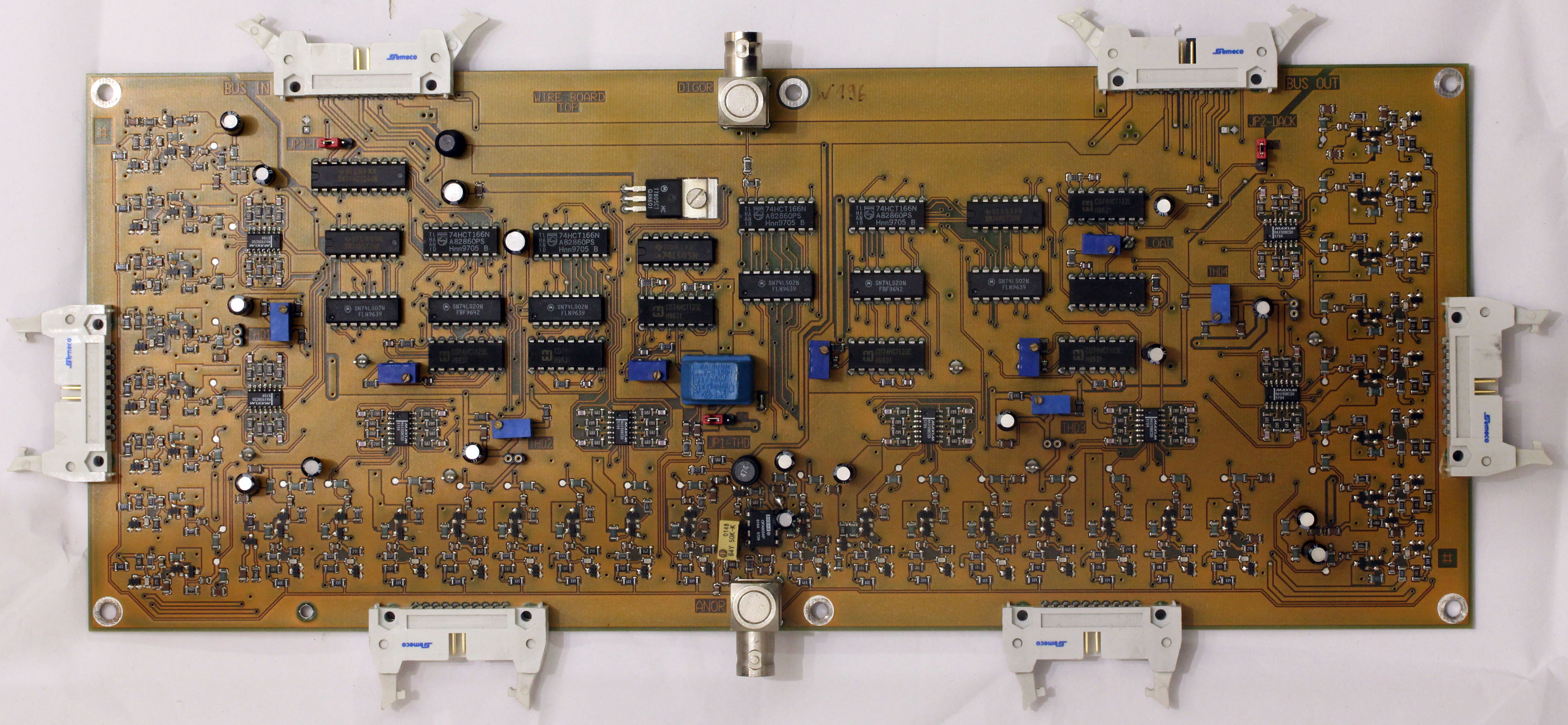
Thanks to cpresser for contributing this wonderfully photographed circuit board as this month’s entry.
January 4, 2023
Non-Destructive Silicon Imaging (and Winner of Name that Ware December 2022)
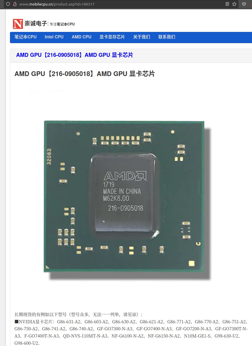
The ware for December 2022 is an AMD Radeon RX540 chip, part number 216-0905018. Congrats to SAM for guessing the ware; email me for your prize. The image is from Fritzchen Fritz’s Flickr feed; I recommend checking out his photos (or you can follow him on twitter). Even if you aren’t into photos of chips, he elevates it to an art. Even more amazingly, all of his work is public domain; hats off to him for contributing these photos to the commons with such a generous license, because it is not easy to prepare the material and take images of this quality. If any of my readers happens to know him and are willing to make an introduction, I’d appreciate that. I only discovered his work by chance while doing some background research.
First, here is the entire photo from which the ware was cropped:
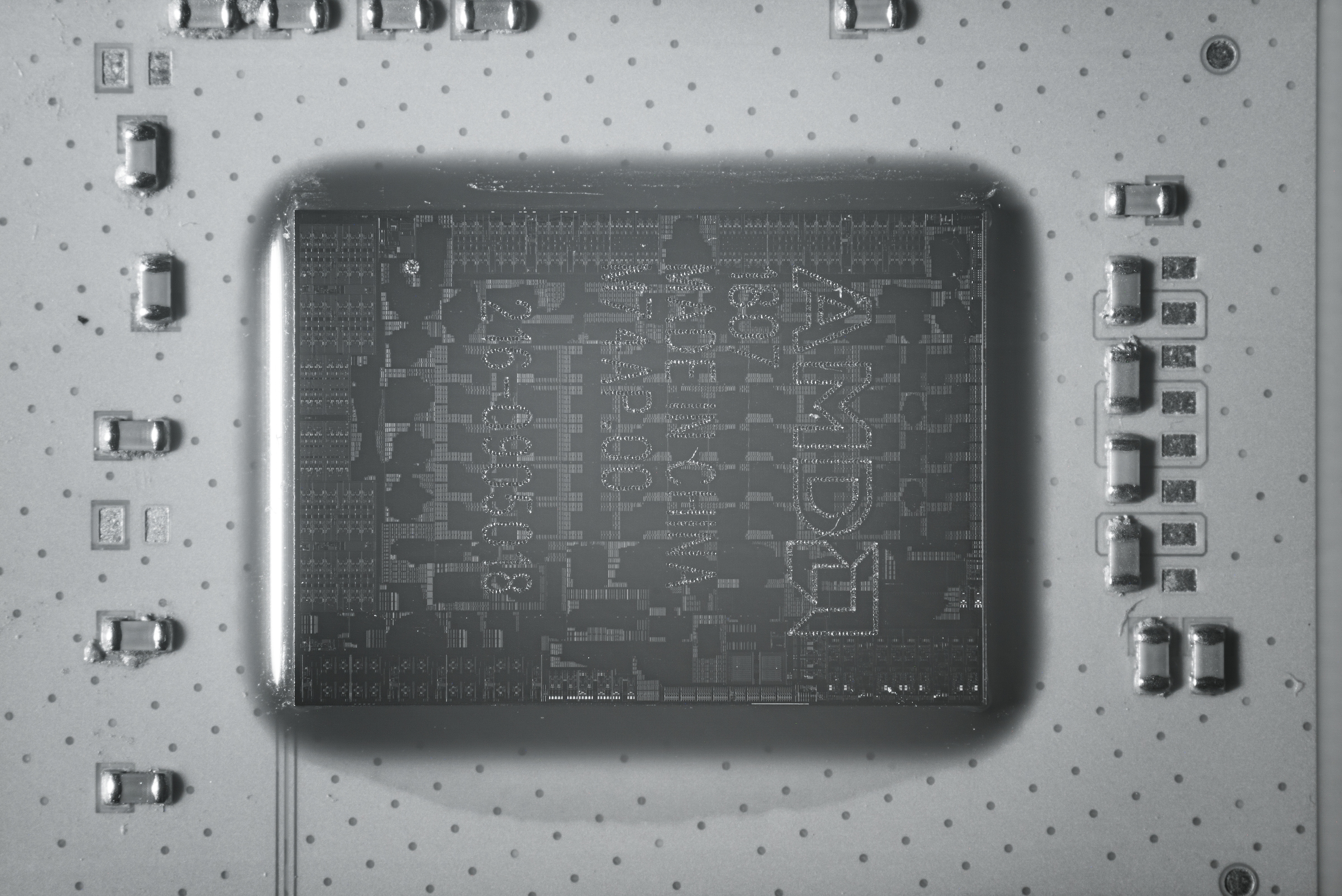
Credit: Fritzchen Fritz
Interestingly, you can see the design of the chip in this photograph. This is not photoshop; based on the notes accompanying the photo, this was taken in “NIR”, or near-infrared, using a Sony NEX-5T.
Silicon is transparent to IR, and so, photographs taken in infra-red can be used to verify, at a coarse level, the construction of a chip!
I was pretty excited to see photos like this posted on the Internet, at full-resolution, because I have only read about this technique in journal articles. Silicon becomes very transparent in infrared:
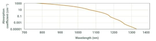
Silicon’s absorption of light in the near infrared range. A lower value is more transparent. Generated using PV lighthouse.
This principle forms the foundation of my efforts to verify the construction of silicon in a non-destructive fashion.
The line between NIR/SWIR (near/shortwave infrared) depends on who you ask, but according to Edmud Optics, it places the line at 1000nm. By this definition, I’m inferring that the above photograph was probably taken using a powerful 900nm illuminator positioned to the left of the chip near the horizon. A bright light at that wavelength would have sufficient power to penetrate the ~1mm thickness of silicon to image the circuits on the other side, and placing it near the horizon prevents swamping the sensor with reflected light except for the bits of metal that happen to catch the light and reflect it upwards.
It’s also possible to do this with a SWIR sensor, using a wavelength closer to 1300nm (where silicon is as transparent as glass is to visible light), but the resolution of the photographs are much higher than the best SWIR sensor that I’m aware of. Unfortunately, it seems all interesting technologies are regulated by the US government’s ITAR, and SWIR area-scan sensors are no exception. I’m guessing they are also a critical component of night vision gear, and thus it is hard to obtain such sensors without a license. Regardless, even the photos taken at 900nm are a powerful demonstration of the utility of IR for inspecting the construction of silicon.
Here’s another image taken using what looks like the same technique:
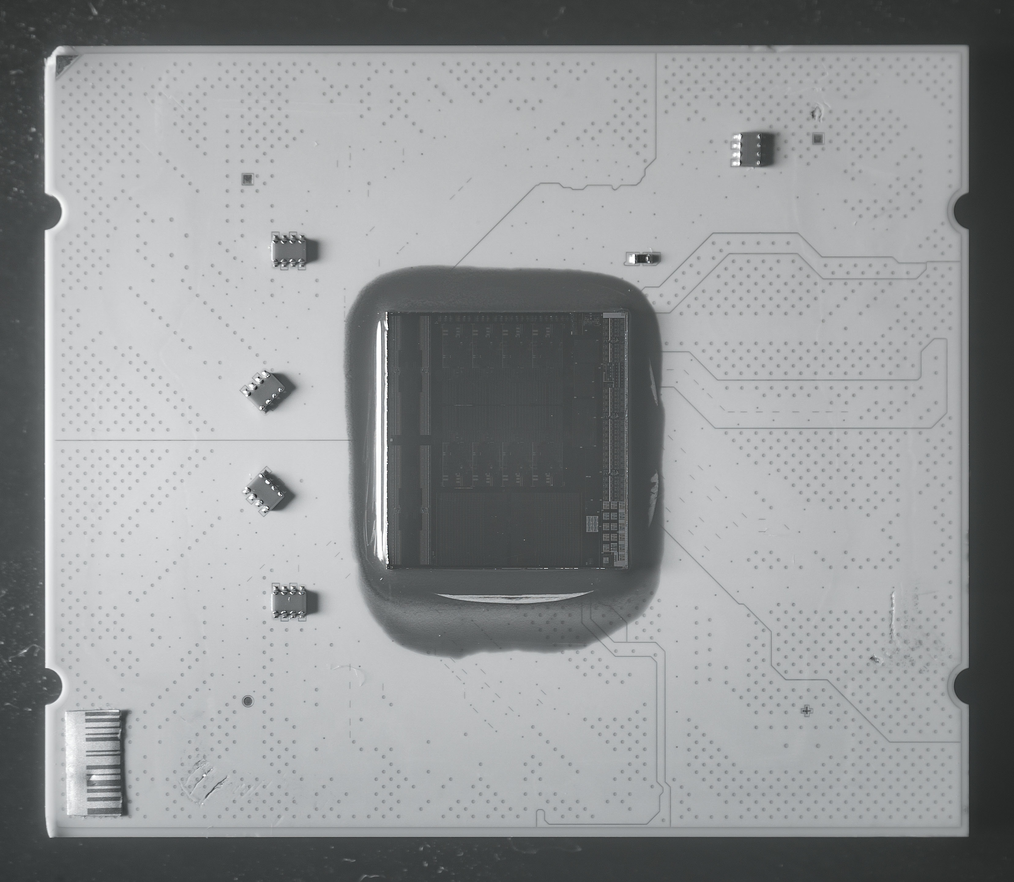
Credit: Fritzchen Fritz
This is of the Via Centaur CHA, which has an excellently detailed Wikichip page complete with floorplans, such as the one shown below.
Credit: Wikichip
Remember, the IR image is from the back side of the die, so you have to mirror-image (and rotate) the front-side floorplan in your head to line it up with orientation of the photograph.
According to Wikichip, this is a TSMC 16FFC (16nm) process, with a 194mm^2 die area. This means the die above is about 13.9 mm on a side. The image as-is (which is 90% package and 10% die) resolves at about 18um/pixel, so perhaps if it was a die-only shot we could resolve at something close to 5um/pixel in a single image.
With image stitching, the resolution can be even higher:
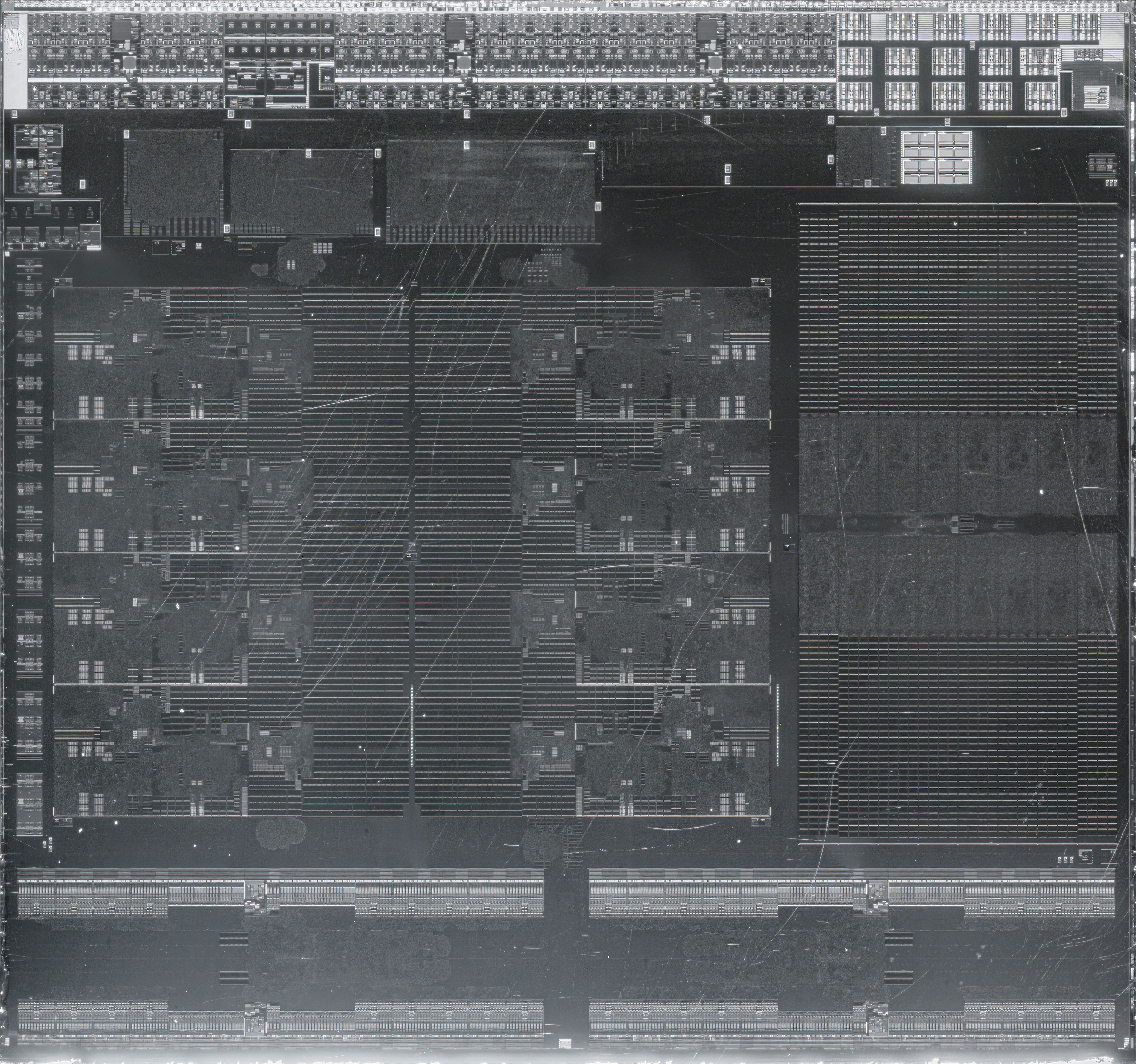
Credit: Fritzchen Fritz
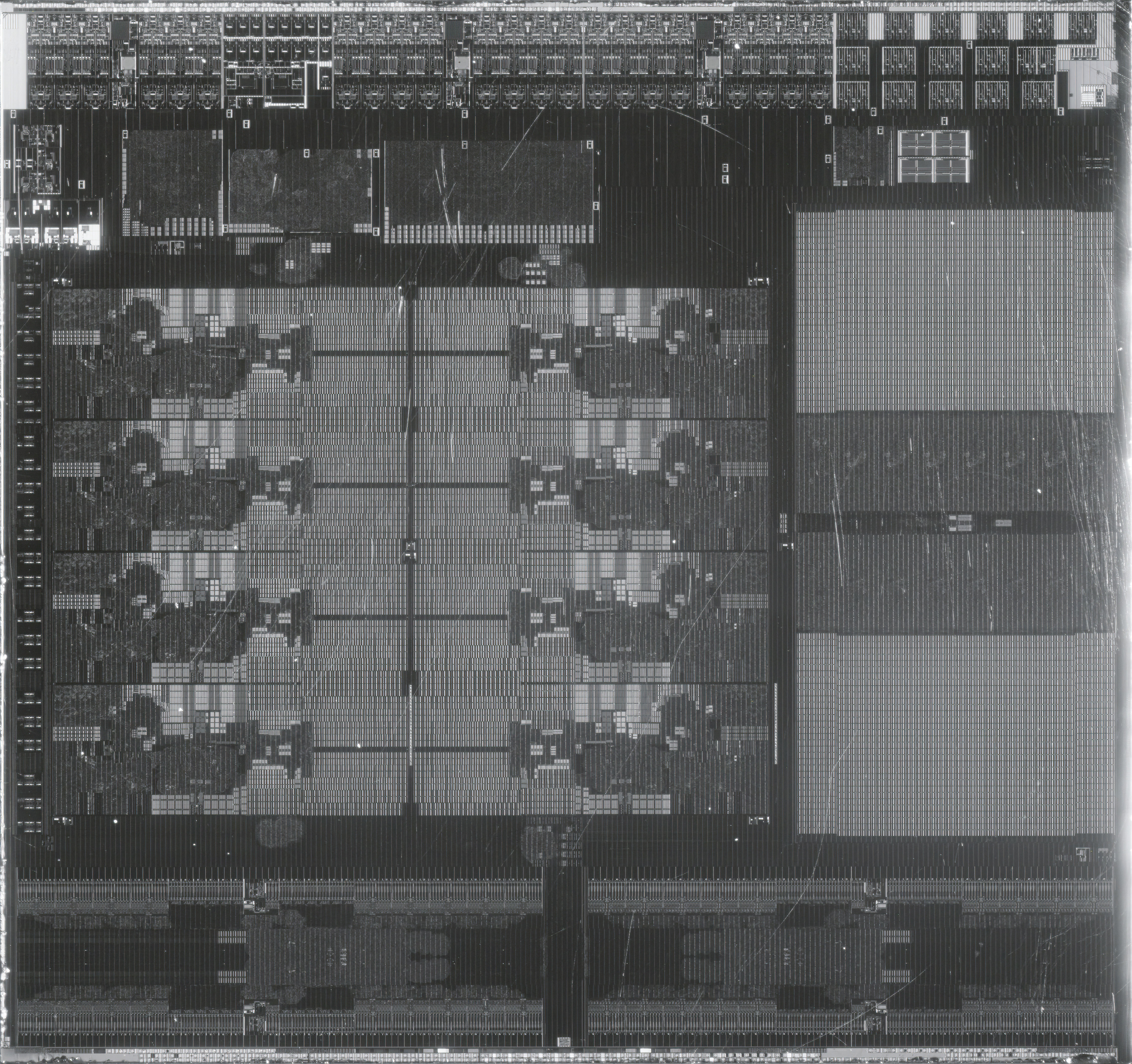
Credit: Fritzchen Fritz
In these two photos, it seems the light source was rotated 90 degrees with respect to the chip, so that different sets of components are highlighted, depending on the bias of the metal routes for that component. Note that I’m inferring this image is taken through the back side because of the presence of scratches that would be from the exposed surface of the silicon, and the orientation of the imaged die is consistent with a back-side shot.
The resolution of the above images boils down to about 3um/pixel — getting fairly close to the limit of what you can do with NIR light. To put this in perspective, TSMC 16FFC has minimum metal pitch of 64nm, so a 9-track standard cell would be 0.576um tall, and an SRAM bitcell has a size of 0.074um^2, so one pixel encompasses roughly 25 logic gates or 120 bits of SRAM. In these images, you can clearly make out variations in the density of standard cell logic, as well as the size and location of individual memory macros; the internal structure of the PCI-express drivers is also readily apparent.
I’ve been contemplating silicon supply chain attacks quite a bit, and I think that at this resolution, one can rule out the following forms of silicon supply chain attacks:
Replacement of the chip with an entirely different design that emulates the originalInsertion of a ROM larger than a few hundred bits containing alternate microcode or instruction codingsInsertion of a RAM macro for recording data — probably of any practical size for a RAM macro, due to the presence of line drivers/amplifiers creating a high-signal reflectionInsertion of extra I/O driversPotential detection of extra eFuse elementsLikely able to detect recompilation/resynthesis of standard cell blobsThis significantly constrains the types of attacks one has to worry about. Without backside imaging and just looking at the exterior package, it’s difficult to even know if a chip has been wholesale replaced for an inferior clone or an emulated version. The inability to add significant amounts of microcode ROM or RAM constrains the types of modifications one could make to a CPU and “get away with it”; with some additional design-level guard rails and open source RTL I suspect one could virtually eliminate effective CPU instruction-level modifications that doesn’t also introduce ISA-level flaws in every mode of operation that could be easily detected with a software-only test.
I have reasons to suspect that modifications to an eFuse box would be detectable, but because eFuses are carefully guarded black boxes such that even chip designers are not allowed to see their insides, it’s possible that a foundry could just build a back door into every eFuse box and we wouldn’t be able to tell the difference because it would be “normal”.
Finally, depending on the repeatability of the place/route tool, a modification to the RTL that triggers a re-synthesis and place/route could change the gross morphology of the standard cell blob. However, I’m not familiar enough with the latest industry-standard tools to know how big a difference that would create. I imagine there are ways to control the place and route seed so that results look very similar if only small changes are made to the RTL, such as inserting a patch wire on a single bit in a non-congested region of a design. However, a larger change, such as the insertion of a 64-bit sampling register in the datapath somewhere, would likely be detectable with this level of imaging.
There’s still a class of exploits that could be undetected with this level of imaging. This would include:
Small changes to test access paths; for example, patching existing ATPG scan chain logic to an existing but unused point on an I/O mux hard macro. This could facilitate unrestricted access to internal state with some additional off-chip circuitry.Spare cell-only modifications that are manually patched using higher metal levels. These patches would be obscured from the back side due to masking by lower metal layers, and by definition no additional transistors are involved.Dopant-level attacks, where transistor flavor or threshold voltages are modified, perhaps to bias a random number generator or to modify the function of a single gate.Other careful modifications that disturb fewer than ~100 logic gates or ~100 bits of SRAM.However, the attack surface of concern is by far smaller with this level of imaging than the current state-of-practice, which consists of squinting at the top markings on a chip package.
My hope for supply chain verification is that end users can establish a practical amount of trust in silicon chips through a combination of imaging and design analysis, without requiring a fully-open PDK (although it certainly is easier and better if the PDK is open). The missing link is an automated imager that can produce results similar to the ones demonstrated by Fritzchens Fritz. These images can then be compared against die shots released by the designer. These die shots would be low enough resolution to not violate foundry NDA, but still have enough detail to constrain the intended positions of blocks. The remaining verification gap (on the order of hundreds of gates / hundreds of bits of SRAM) could be filled in with design techniques that harden against small exploit vectors, perhaps by the use of redundant/byzantine fault tolerant logic, or by some combination of inducing faults and scan chain analysis to confirm correct construction at the gate level. And finally, open source RTL is required to help establish a link between what is visible, and what was intended by the designer (and of course also to help discover any bugs/backdoors introduced by the designer).
And now back to the Name that Ware competition. Confusingly, one of the first answers in the comments points to a tweet that also claims to have taken the photo. I did a bit of poking about and the image appears to be identical to the one on Fritzchen Fritz’s feed, down to the position of solder particulates and lint. There’s a number of possible explanations for this; I won’t speculate as to what is going on, but I will comment that the chip is not typically referred to as an “AMD M74AP” — M74AP is the lot code, so I couldn’t declare Taylan the winner, unfortunately (so close, though!). 216-0905018 is the canonical part number; if you search around for the part number, you will see several examples of chips that have the same part number, but a different lot code. This one, for example, has a lot code of M62K8.00.
PostscriptWhen going through Fitzchen Fritz’s photos, I was also considering using this image as the Name that Ware:
Credit: Fritzchen Fritz
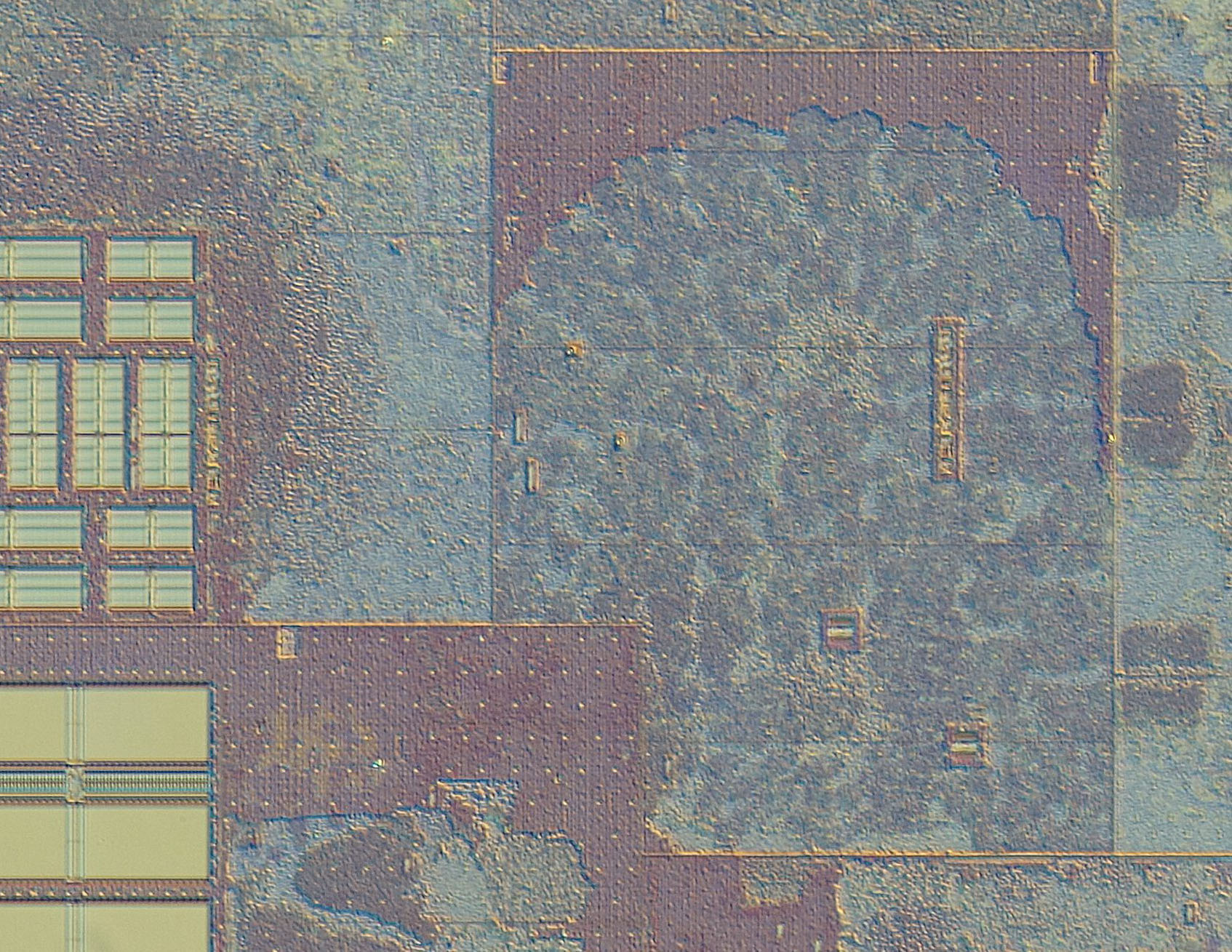
It’s a tiny portion (1/400th the area) of an Intel i3-8121U (187MiB full-res mirror link), fabbed in a 10nm process. The region is cropped from a section centered in the top right quadrant of the image.
In terms of actual dimensions, the region is about 485um x 375um if I’ve done my math right – about the area covered by a medium sand particle. According to Wikichip, a 9-track standard cell would be 0.324um high, so if the area were covered with nothing but square 9-track standard cells, it would hold 1500 x 1150 cells (1.7M cells, or about one gate per pixel in the photo), or 700kiB of the densest SRAM cells (without sense amps etc.)
However, the area is not homogeneously covered with one or the other, and in fact has lots of unused silicon. The darker purplish regions are unused silicon — for one reason or the other (often times routing/floorplanning constraints, and sometimes schedule constraints), there are no logic transistors there. I think only the solid tan regions in the lower left hand corners contain high density SRAM cells; the smaller rectangles above them could contain SRAM, but could also be some other type of memory more optimized for performance or port count.
Each SRAM region is divided by sense amps and other driver logic. One solid, SRAM-cell-only region is about 48.7×28.7um, which is about 5.4kiB, so the overall region of larger rectangles holds about 22kiB of memory, including an overhead of about 35% for the drivers and amps. Likewise, the cauliflower-like structure in the center is about 750 gates wide by 900 gates high (if the gates were square — which they aren’t, so this is an upper bound), or about 600k gates (again, this image is at a resolution of about 1 pixel/gate). That would fit about a dozen VexRiscv cores, or a few 80486’s, so it’s not a small chunk of logic.
Finally, I think (but am not sure) that the rectangular cut-out regions within the cauliflower-region are clock drivers or repeaters. No transistors are placed in the trench around them probably to meet thermal flux constraints, and I also wouldn’t be surprised if they packed some local decoupling capacitors around the drivers using dummy transistors and/or MIM capacitors to reduce power droop and induced jitter in that region.
What I love about this image is how clouds of standard cells take on organic shapes when viewed at this resolution. To me it looks more like mold or bacteria growing in a petri dish than the pinnacle of precision manufactured goods. But perhaps this is just convergent evolution in action, driven by the laws of physics: signals diffuse through on-chip wires, much like nutrients in a media.
December 31, 2022
Name that Ware, December 2022
The Ware for December 2022 is shown below.
Turning this into a suitable Name that Ware-style entry was a bit tough, but I think maybe I hit a balance between leaving enough clues, and giving it away. We’ll see shortly!
I have a lot more to say about this ware: I will give proper attribution once the ware has been guessed (or the end of the month, whichever is sooner); but let’s just say I was incredibly pleased to find such detailed images in the public domain.
Winner, Name that Ware November 2022
The ware for November 2022 is a Keithley 2110-240. I’ll give Rodrigo F. the win, but I’m curious how he knew it was the -240 version; I did not expect someone to discern the line voltage rating from the photos!
Also, thank you Ian Mason for the lucid explanation of the exposed traces near key signals. Here’s his quoted answer, so you don’t have to look it up in the comment thread:
The reason for stripping resist from over guard rings [is] to ensure that any leakage paths come into electrical contact with the guard ring. If you had, say, a bit of flux residue as a leakage path, if it passed between two pins but over the solder mask then the guard ring would be insulated from it and would have no effect. The whole point of a guard ring is that it’s a (relatively) low impedance path either to ground or to a duplicate of the measured signal – being insulated behind soldermask is anything but low impedance.
It’s tricks like these they never teach you in school. I’m guessing it was a hard-learned lesson for the persons who had to figure out that trick on their own. Thanks for sharing the knowledge!
December 19, 2022
Towards a More Open Secure Element Chip
“Secure Element” (SE) chips have traditionally taken a very closed-source, NDA-heavy approach. Thus, it piqued my interest when an early-stage SE chip startup, Cramium (still in stealth mode), approached me to advise on open source strategy. This blog post explains my reasoning for agreeing to advise Cramium, and what I hope to accomplish in the future.
As an open source hardware activist, I have been very pleased at the progress made by the eFabless/Google partnership at creating an open-to-the-transistors physical design kit (PDK) for chips. This would be about as open as you can get from the design standpoint. However, the partnership currently supports only lower-complexity designs in the 90nm to 180nm technology nodes. Meanwhile, Cramium is planning to tape out their security chip in the 22nm node. A 22nm chip would be much more capable and cost-effective than one fabricated in 90nm (for reference, the RP2040 is fabricated in 40nm, while the Raspberry Pi 4’s CPU is fabricated in 28nm), but it would not be open-to-the-transistors.
Cramium indicated that they want to push the boundaries on what one can do with open source, within the four corners of the foundry NDAs. Ideally, a security chip would be fabricated in an open-PDK process, but I still feel it’s important to engage and help nudge them in the right direction because there is a genuine possibility that an open SDK (but still closed PDK) SE in a 22nm process could gain a lot of traction. If it’s not done right, it could establish poor de-facto standards, with lasting impacts on the open source ecosystem.
For example, when Cramium approached me, their original thought was to ship the chip with an ARM Cortex M7 CPU. Their reasoning is that developers prize a high-performance CPU, and the M7 is one of the best offerings in its class from that perspective. Who doesn’t love a processor with lots of MHz and a high IPC?
However, if Cramium’s chip were to gain traction and ship to millions of customers, it could effectively entrench the ARM instruction set — and more importantly — quirks such as the Memory Protection Unit (MPU) as the standard for open source SEs. We’ve seen the power of architectural lock-in as the x86 serially shredded the Alpha, Sparc, Itanium and MIPS architectures; so, I worry that every new market embracing ARM as a de-facto standard is also ground lost to fully open architectures such as RISC-V.
So, after some conversations, I accepted an advisory position at Cramium as the Ecosystem Engineer under the condition that they also include a RISC-V core on the chip. This is in addition to the Cortex M7. The good news is that a RISC-V core is royalty-free, and the silicon area necessary to add it at 22nm is basically a rounding error in cost, so it was a relatively easy sell. If I’m successful at integrating the RISC-V core, it will give software developers a choice between ARM and RISC-V.
So why is Cramium leaving the M7 core in? Quite frankly, it’s for risk mitigation. The project will cost upwards of $20 million to tape out. The ARM M7 core has been taped out and shipped in millions of products, and is supported by a billion-dollar company with deep silicon experience. The VexRiscv core that we’re planning to integrate, on the other hand, comes with no warranty of fitness, and it is not as performant as the Cortex M7. It’s just my word and sweat of brow that will ensure it hopefully works well enough to be usable. Thus, I find it understandable that the people writing the checks want a “plan B” that involves a battle-tested core, even if proprietary.
This will understandably ruffle the feathers of the open source purists who will only certify hardware as “Free” if and only if it contains solely libre components. I also sympathize with their position; however, our choices are either the open source community somehow provides a CPU core with a warranty of fitness, effectively underwriting a $20 million bill if there is a fatal bug in the core, or I walk away from the project for “not being libre enough”, and allow ARM to take the possibly soon-to-be-huge open source SE market without challenge.
In my view it’s better to compromise and have a seat at the table now, than to walk away from negotiations and simply cede green fields to proprietary technologies, hoping to retake lost ground only after the community has achieved consensus around a robust full-stack open source SE solution. So, instead of investing time arguing over politics before any work is done, I’m choosing to invest time building validation test suites. Once I have a solid suite of tests in hand, I’ll have a much stronger position to argue for the removal of any proprietary CPU cores.
On the Limit of Openness in a Proprietary EcosystemAdvising on the CPU core is just one of many tasks ahead of me as their open source Ecosystem Engineer. Cramium’s background comes from the traditional chip world, where NDAs are the norm and open source is an exotic and potentially fatal novelty. Fatal, because most startups in this space exit through acquisition, and it’s much harder to negotiate a high acquisition price if prized IP is already available free-of-charge. Thus my goal is to not alienate their team with contumelious condescension about the obviousness and goodness of open source that is regrettably the cultural norm of our community. Instead, I am building bridges and reaching across the aisle, trying to understand their concerns, and explaining to them how and why open source can practically benefit a security chip.
To that end, trying to figure out where to draw the line for openness is a challenge. The crux of the situation is that the perceived fear/uncertainty/doubt (FUD) around a particular attack surface tends to have an inverse relation to the actual size of the attack surface. This illustrates the perceived FUD around a given layer of the security hierarchy:
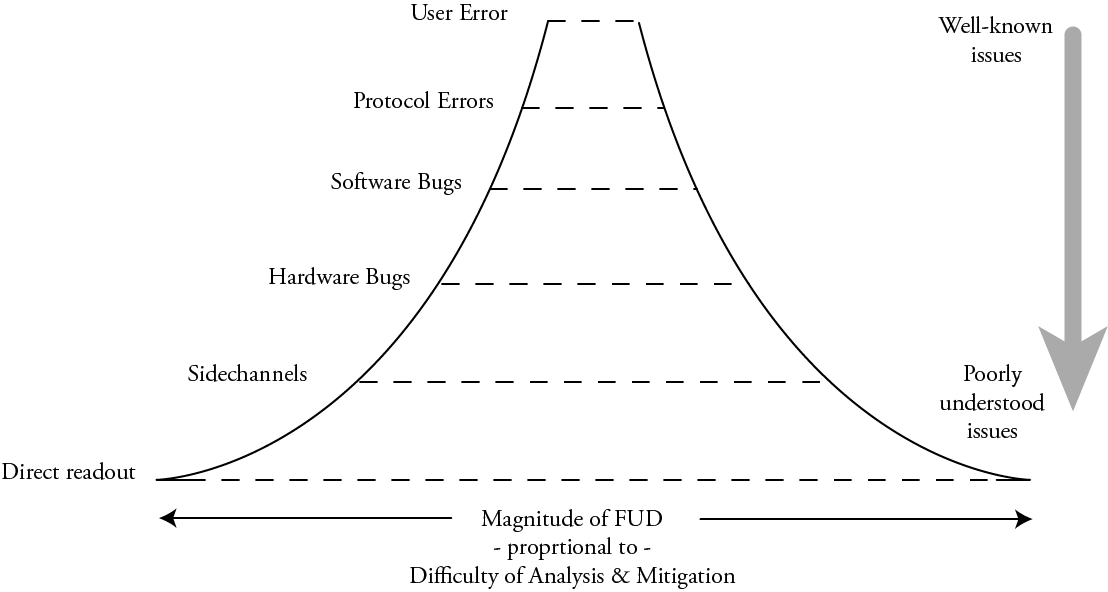
Generally, the amount of FUD around an attack surface grows with how poorly understood the attack surface is: naturally we fear things we don’t understand well; likewise we have less fear of the familiar. Thus, “user error” doesn’t sound particularly scary, but “direct readout” with a focused ion beam of hardware security keys sounds downright leet and scary, the stuff of state actors and APTs, and also of factoids spouted over beers with peers to sound smart.
However, the actual size of the attack surface is quite the opposite:
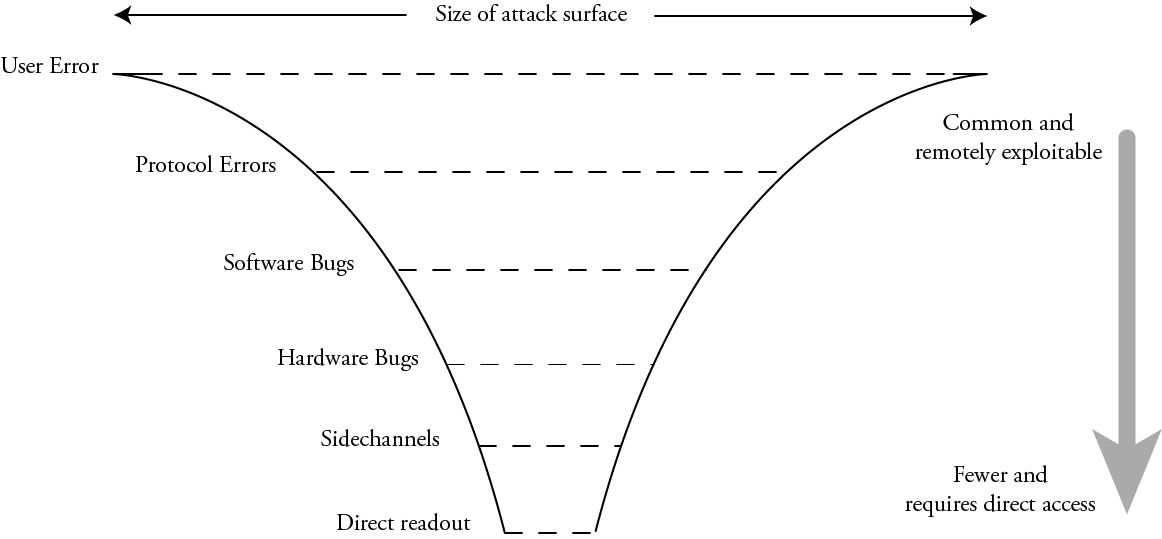
In practice, “user error” – weak passwords, spearphishing, typosquatting, or straight-up fat fingering a poorly designed UX – is common and often remotely exploitable. Protocol errors – downgrade attacks, failures to check signatures, TOCTOUs – are likewise fairly common and remotely exploitable. Next in the order are just straight-up software bugs – buffer overruns, use after frees, and other logic bugs. Due to the sheer volume of code (and more significantly the rate of code turnover) involved in most security protocols, there are a lot of bugs, and a constant stream of newly minted bugs with each update.
Beneath this are the hardware bugs. These are logical errors in the implementation of a function of a piece of hardware, such as memory aliasing, open test access ports, and oversights such as partially mutable cryptographic material (such as an AES key that can’t be read out, but can be updated one byte at a time). Underneath logical hardware bugs are sidechannels – leakage of secret information through timing, power, and electromagnetic emissions that can occur even if the hardware is logically perfect. And finally, at the bottom layer is direct readout – someone with physical access to a chip directly inspecting its arrangement of atoms to read out secrets. While there is ultimately no defense against the direct readout of nonvolatile secrets short of zeroizing them on tamper detection, it’s an attack surface that is literally measured in microns and it requires unmitigated physical access to hardware – a far cry from the ubiquity of “user error” or even “software bugs”.
The current NDA-heavy status quo for SE chips creates an analytical barrier that prevents everyday users like us from determining how big the actual attack surface is. That analytical barrier actually extends slightly up the stack from hardware, into “software bugs”. This is because without intimate knowledge of how the hardware is supposed to function, there are important classes of software bugs we can’t analyze.
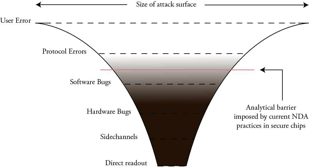
Furthermore, the inability of developers to freely write code and run it directly on SEs forces more functionality up into the protocol layer, creating an even larger attack surface.
My hope is that working with Cramium will improve this situation. In the end, we won’t be able to entirely remove all analytical barriers, but hopefully we arrive at something closer to this:

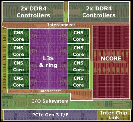
Due to various NDAs, we won’t be able to release things such as the mask geometries, and there are some blocks less relevant to security such as the ADC and USB PHY that are proprietary. However, the goal is to have the critical sections responsible for the security logic, such as the cryptographic accelerators, the RISC-V CPU core, and other related blocks shared as open source RTL descriptions. This will allow us to have improved, although not perfect, visibility into a significant class of hardware bugs.
The biggest red flag in the overall scenario is that the on-chip interconnect matrix is slated to be a core generated using the ARM NIC-400 IP generator, so this logic will not be available for inspection. The reasoning behind this is, once again, risk mitigation of the tapeout. This is unfortunate, but this also means we just need to be a bit more clever about how we structure the open source blocks so that we have a toolbox to guard against potential misbehavior in the interconnect matrix.
My personal goal is to create a fully OSS-friendly FPGA model of the RISC-V core and their cryptographic accelerators using the LiteX framework, so that researchers and analysts can use this to model the behavior of the SE and create a battery of tests and fuzzers to confirm the correctness of construction of the rest of the chip.
In addition to the work advising Cramium’s engagement with the open source community, I’m also starting to look into non-destructive optical inspection techniques to verify chips in earnest, thanks to a grant I received from NLNet’s NGI0 Entrust fund. More on this later, but it’s my hope that I can find a synergy between the work I’m doing at Cramium and my silicon verification work to help narrow the remaining gaps in the trust model, despite refractory foundry and IP NDAs.
Counterpoint: The Utility of Secrecy in SecuritySecrecy has utility in security. After all, every SE vendor runs with this approach, and for example, we trust the security of nuclear stockpiles to hardware that is presumably entirely closed source.
Secrecy makes a lot of sense when:
Even a small delay in discovering a secret can be a matter of life or deathDistribution and access to hardware is already strictly controlledThe secrets would rather be deleted than discoveredMilitary applications check all these boxes. The additional days, weeks or months delay incurred by an adversary analyzing around some obfuscation can be a critical tactical advantage in a hot war. Furthermore, military hardware has controlled distribution; every mission-critical box can be serialized and tracked. Although systems are designed assuming serial number 1 is delivered to the Kremlin, great efforts are still taken to ensure that is not the case (or that a decoy unit is delivered), since even a small delay or confusion can yield a tactical advantage. And finally, in many cases for military hardware, one would rather have the device self-destruct and wipe all of its secrets, rather than have its secrets extracted. Building in booby traps that wipe secrets can measurably raise the bar for any adversary contemplating a direct-readout attack.
On the other hand, SEs like those found in bank cards and phones are:
Widely distributed – often directly and intentionally to potentially adversarial partiesProtecting data at rest (value of secret is constant or may even grow with time)Used as a trust root for complicated protocols that typically update over timeProtecting secrets where extraction is preferable to self-destruction. The legal system offers remedies for recourse and recovery of stolen assets; whereas self-destruction of the assets offers no recourseIn this case, the role of the anti-tamper countermeasures and side-channel minimization is to raise the investment necessary to recover data from “trivial” to somewhere around “there’s probably an easier and cheaper way to go about this…right?”. After all, for most complicated cryptosystems, the bigger risk is an algorithmic or protocol flaw that can be exploited without any circumvention of hardware countermeasures. If there is a protocol flaw, employing an SE to protect your data is like using a vault, but leaving the keys dangling on a hook next to the vault.
It is useful to contemplate who bears the greatest risk in the traditional SE model, where chips are typically distributed without any way to update their firmware. While an individual user may lose the contents of their bank account, a chip maker may bear a risk of many tens of millions of dollars in losses from recalls, replacement costs and legal damages if a flaw were traced to their design issue. In this game, the player with the most to lose is the chipmaker, not any individual user protected by the chip. Thus, a chipmaker has little incentive to disclose their design’s details.
A key difference between a traditional SE and Cramium’s is that Cramium’s firmware can be updated (assuming an updateable SKU is released; this was a surprisingly controversial suggestion when I brought it up). This is thanks in part to the extensive use of non-volatile ReRAM to store the firmware. This likewise shifts the calculus on what constitutes a recall event. The open source firmware model also means that the code on the device comes, per letter of the license, without warranty; the end customer is ultimately responsible for building, certifying and deploying their own applications. Thus, for a player like Cramium, the potential benefits of openness outweigh those of secrecy and obfuscation embraced by traditional SE vendors.
SummaryMy role is to advise Cramium on how to shift the norms around SEs from NDAs to openness. Cramium is not attempting to forge an open-foundry model – they are producing parts using a relatively advanced (compared to your typical stand-alone SE) 22nm process. This process is protected by the highly restrictive foundry NDAs. However, Cramium plans to release much of their design under an open source license, to achieve the following goals:
Facilitate white-box inspection of cryptosystems implemented using their primitivesSpeed up discovery of errors; and perhaps more importantly, improve the rate at which they are patchedReduce the risk of protocol and algorithmic errors, so that hardware countermeasures could be the actual true path of least resistanceBuild trustPromote wide adoption and accelerate application developmentCramium is neither fully open hardware, nor is it fully closed. My goal is to steer it toward the more open side of the spectrum, but the reality is there are going to be elements that are too difficult to open source in the first generation of the chip.
The Cramium chip complements the eFabless/Google efforts to build open-to-the-transistors chips. Today, one can build chips that are open to the mask level using 90 – 180nm processes. Unfortunately, the level of integration achievable with their current technology isn’t quite sufficient for a single-chip Secure Element. There isn’t enough ROM or RAM available to hold the entire application stack on chip, thus requiring a multi-chip solution and negating the HSM-like benefits of custom silicon. The performance of older processes is also not sufficient for the latest cryptographic systems, such as Post Quantum algorithms or Multiparty Threshold ECDSA with Identifiable Aborts. On the upside, one could understand the design down to the transistor level using this process.
However, it’s important to remember that knowing the mask pattern does not mean you’ve solved the supply chain problem, and can trust the silicon in your hands. There are a lot of steps that silicon goes through to go from foundry to product, and at any of those steps the chip you thought you’re getting could be swapped out with a different one; this is particularly easy given the fact that all of the chips available through eFabless/Google’s process use a standardized package and pinout.
In the context of Cramium, I’m primarily concerned about the correctness of the RTL used to generate the chip, and the software that runs on it. Thus, my focus in guiding Cramium is to open sufficient portions of the design such that anyone can analyze the RTL for errors and weaknesses, and less on mitigating supply-chain level attacks.
That being said, RTL-level transparency can still benefit efforts to close the supply chain gap. A trivial example would be using the RTL to fuzz blocks with garbage in simulation; any differences in measured hardware behavior versus simulated behavior could point to extra or hidden logic pathways added to the design. Extra backdoor circuitry injected into the chip would also add loading to internal nodes, impacting timing closure. Thus, we could also do non-destructive, in-situ experiments such as overclocking functional blocks to the point where they fail; with the help of the RTL we can determine the expected critical path and compare it against the observed failure modes. Strong outliers could indicate tampering with the design. While analysis like this cannot guarantee the absence of foundry-injected backdoors, it constrains the things one could do without being detected. Thus, the availability of design source opens up new avenues for verifying correctness and trustability in a way that would be much more difficult, if not impossible, to do without design source.
Finally, by opening as much of the chip as possible to programmers and developers, I’m hoping that we can get the open source SE chip ecosystem off on the right foot. This way, as more advance nodes shift toward open PDKs, we’ll be ready and waiting to create a full-stack open source solution that adequately addresses all the security needs of our modern technology ecosystem.
November 30, 2022
Name that Ware November, 2022
The Ware for November 2022 is shown below.

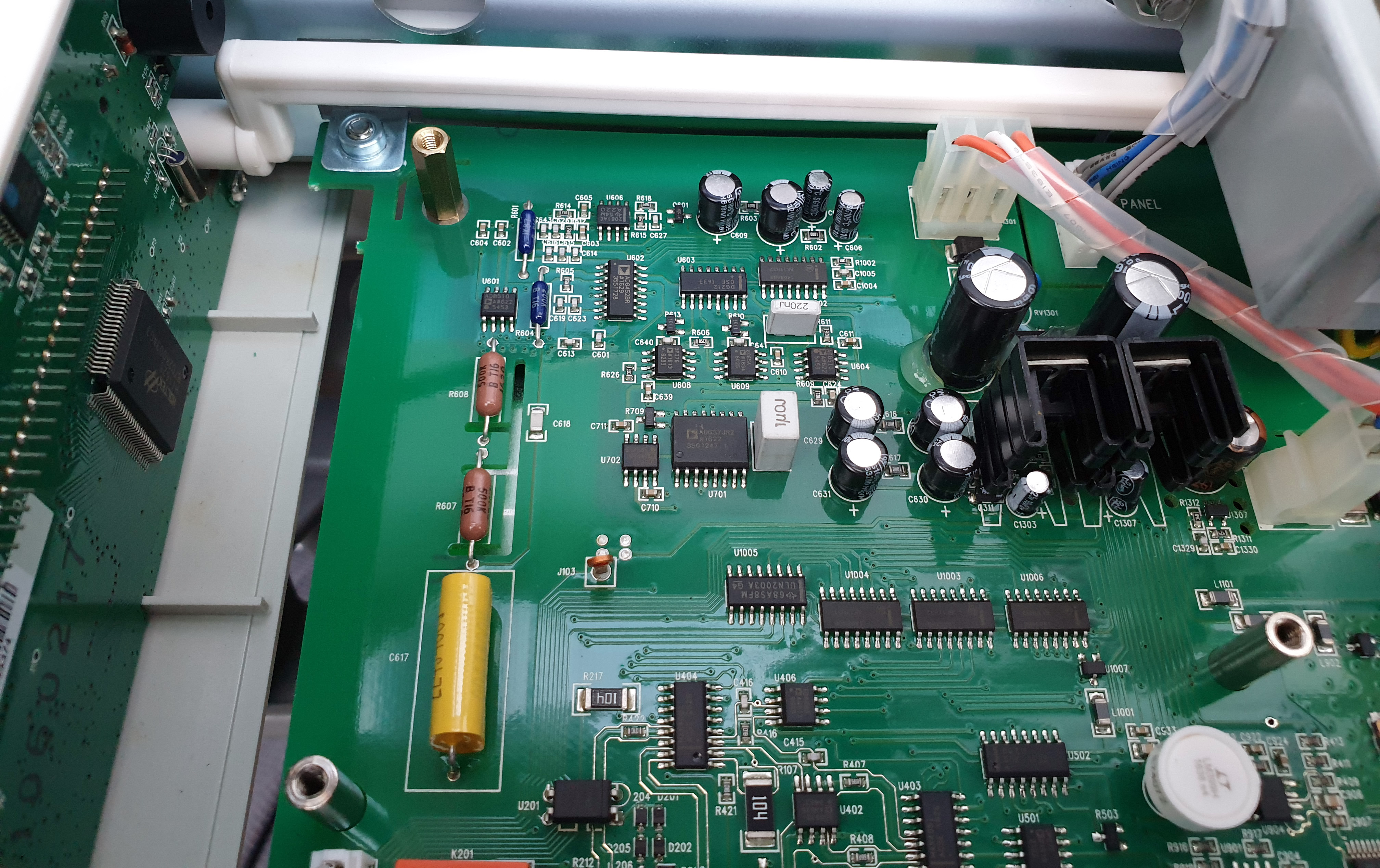
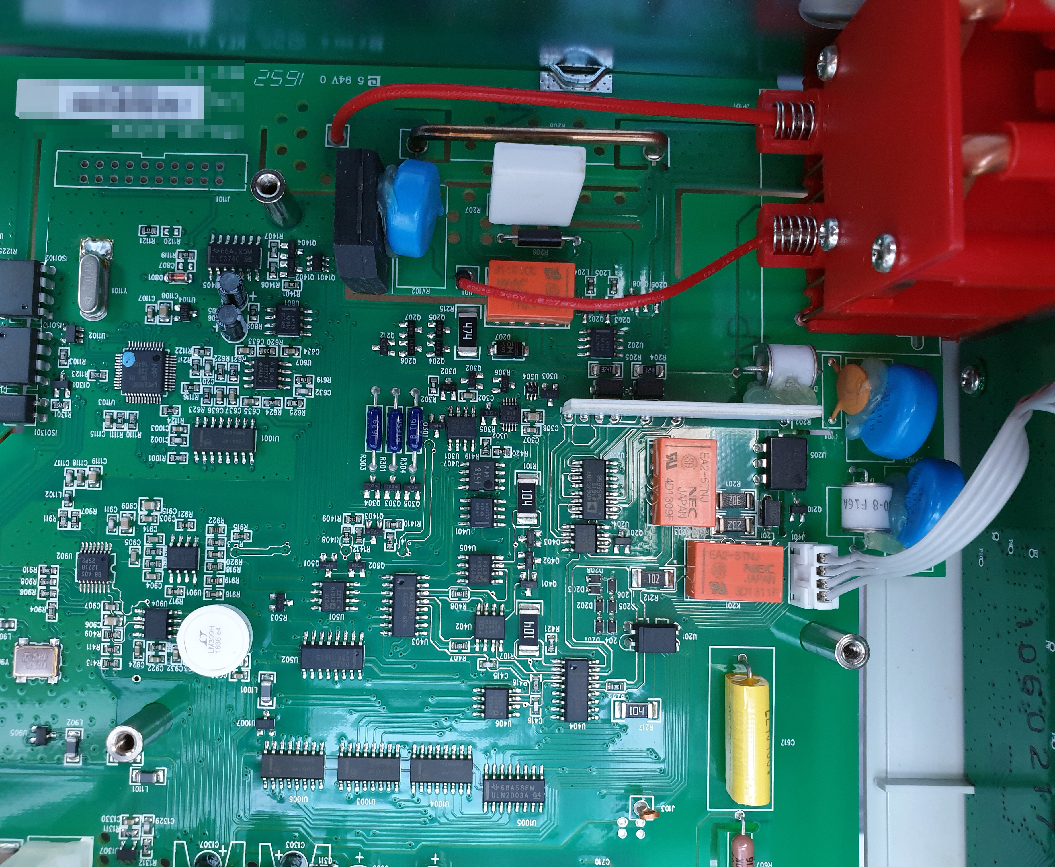

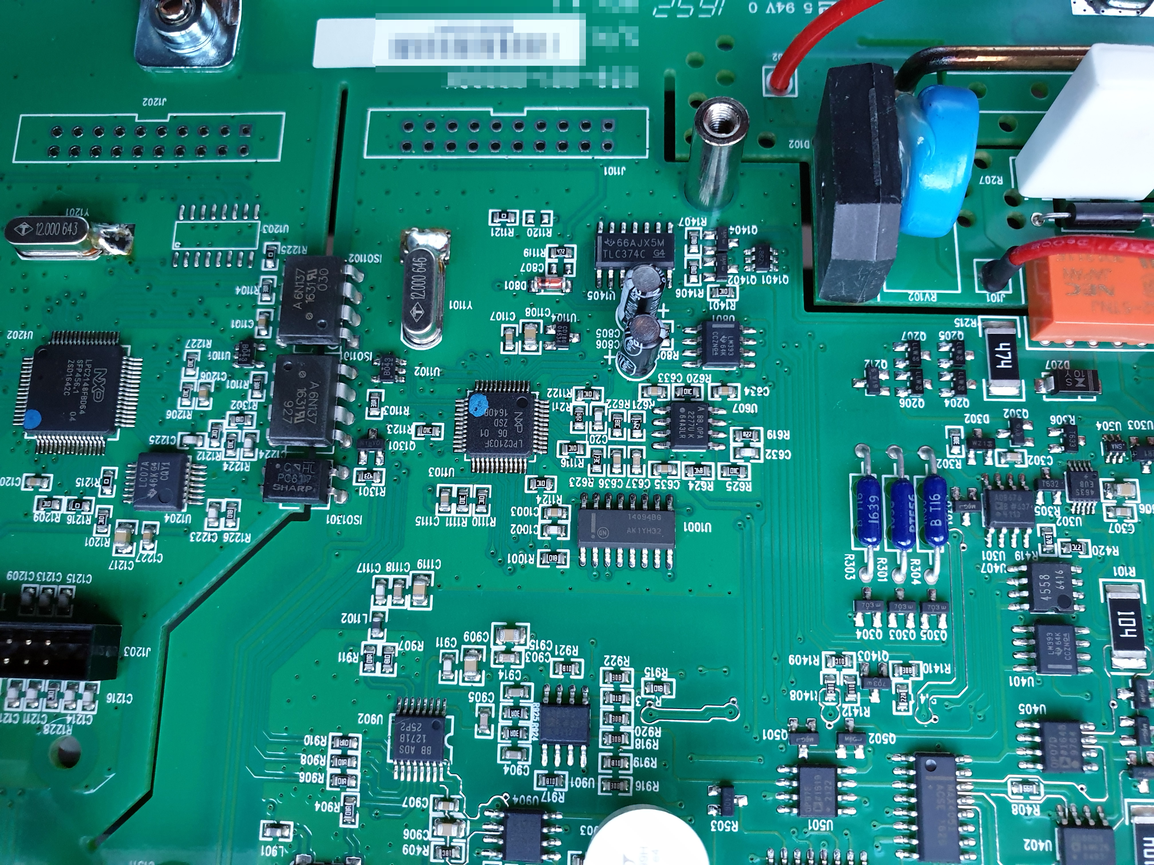
A grounded guard ring is placed around some of the most sensitive analog traces; I would love it if someone could teach me why the soldermask is removed for these guard rings. I imagine there must be some motivation to retain this motif even into mass production, since the mask-less traces run between SMT pins, which I have to imagine incurs a potential yield impact, or at the very least it makes rework more challenging.
Also, yet another tamper-proof seal broken:
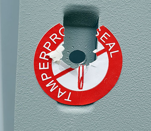
It was just a matter of time…such is the fate of any seal within my reach!
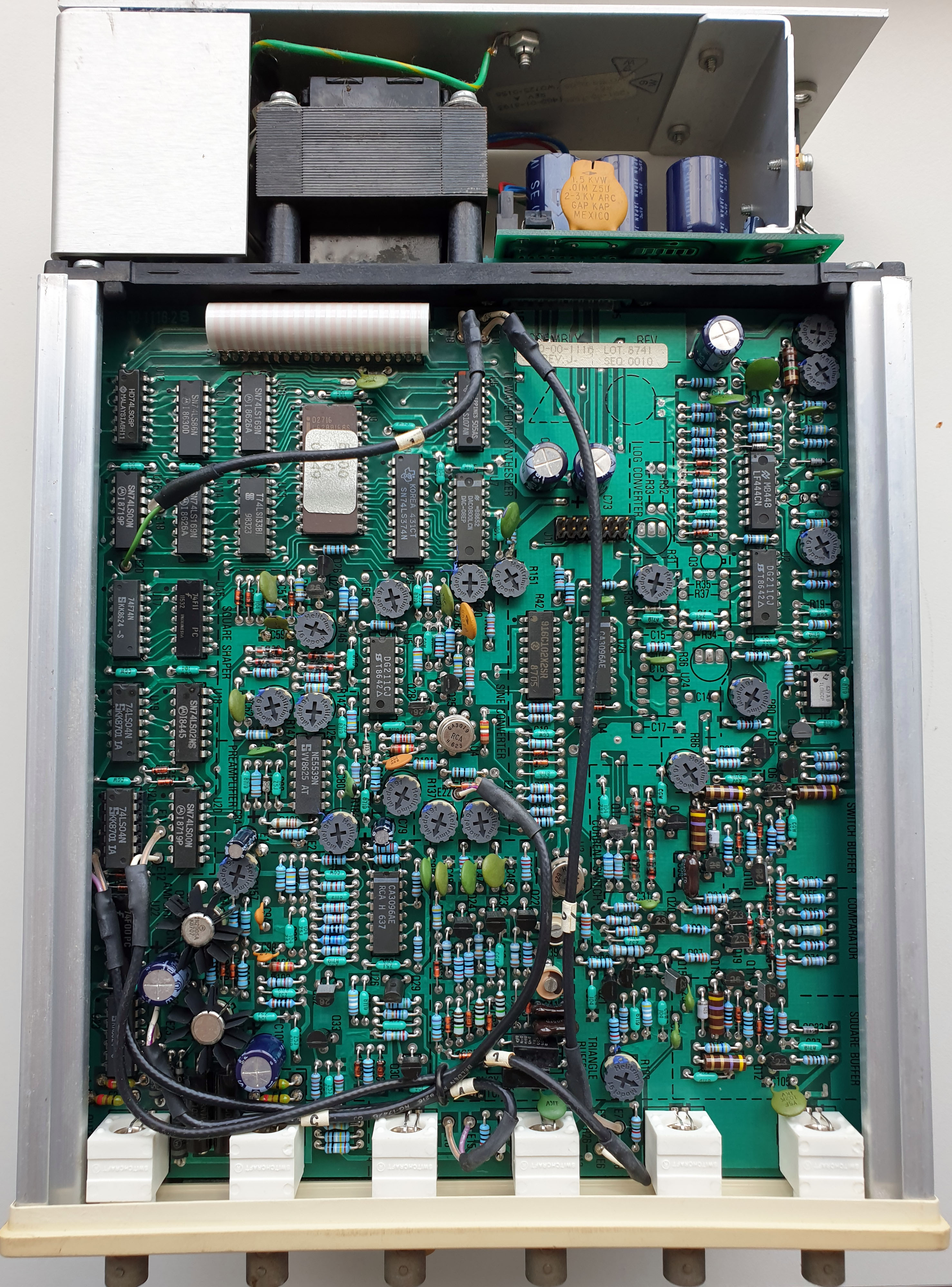
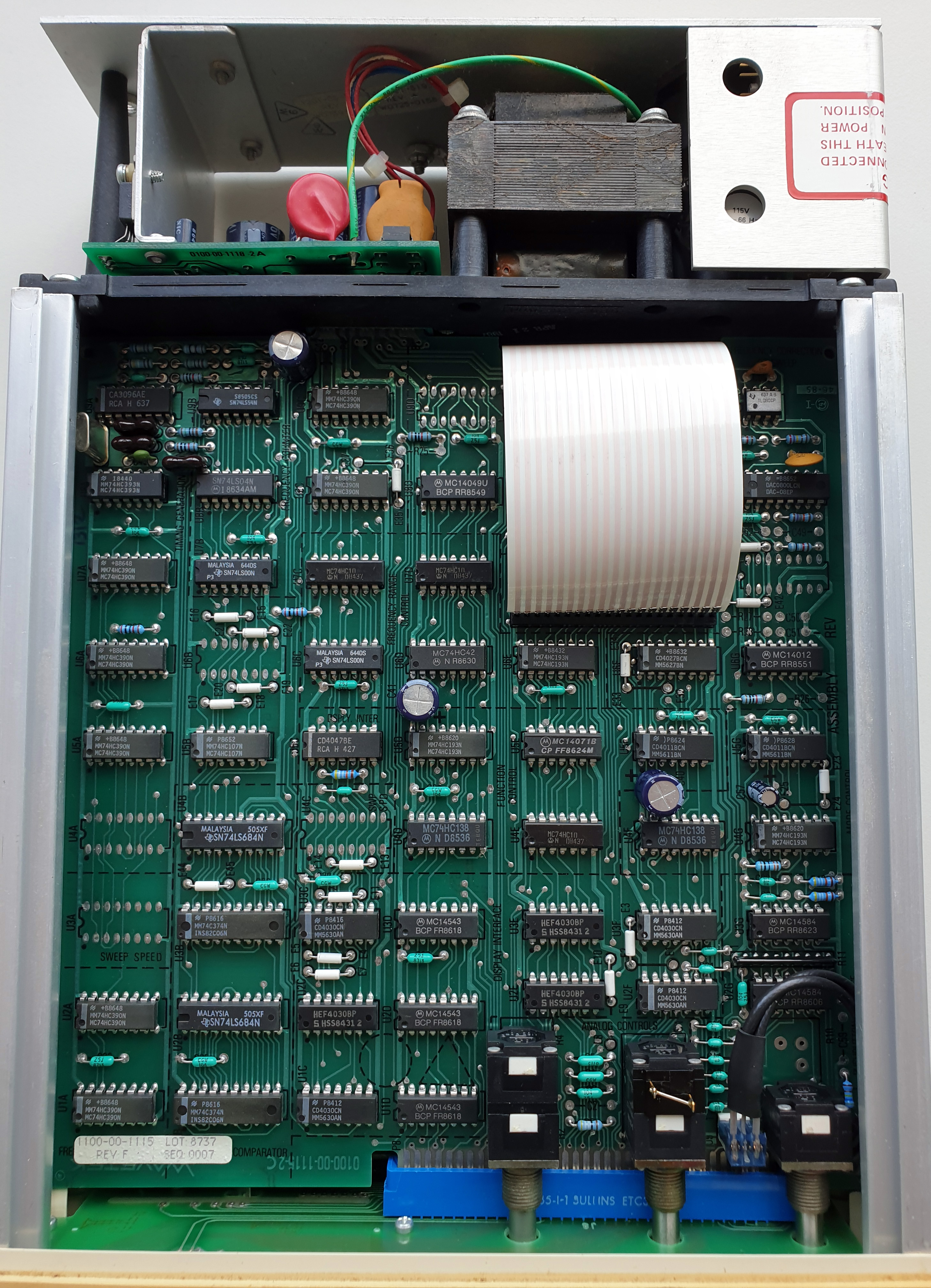
Winner, Name that Ware October 2022
The Ware for October 2022 is a Wavetek Model 21 signal generator. The winner is Marc! Congrats, email me for your prize!
Here’s some more photos of the system for context. It consists of a function generator (analog) board, and a digital control board, along with a third board (not shown) that manages the LCD and buttons.
October 29, 2022
Name that Ware, October 2022
The Ware for October 2022 is shown below.
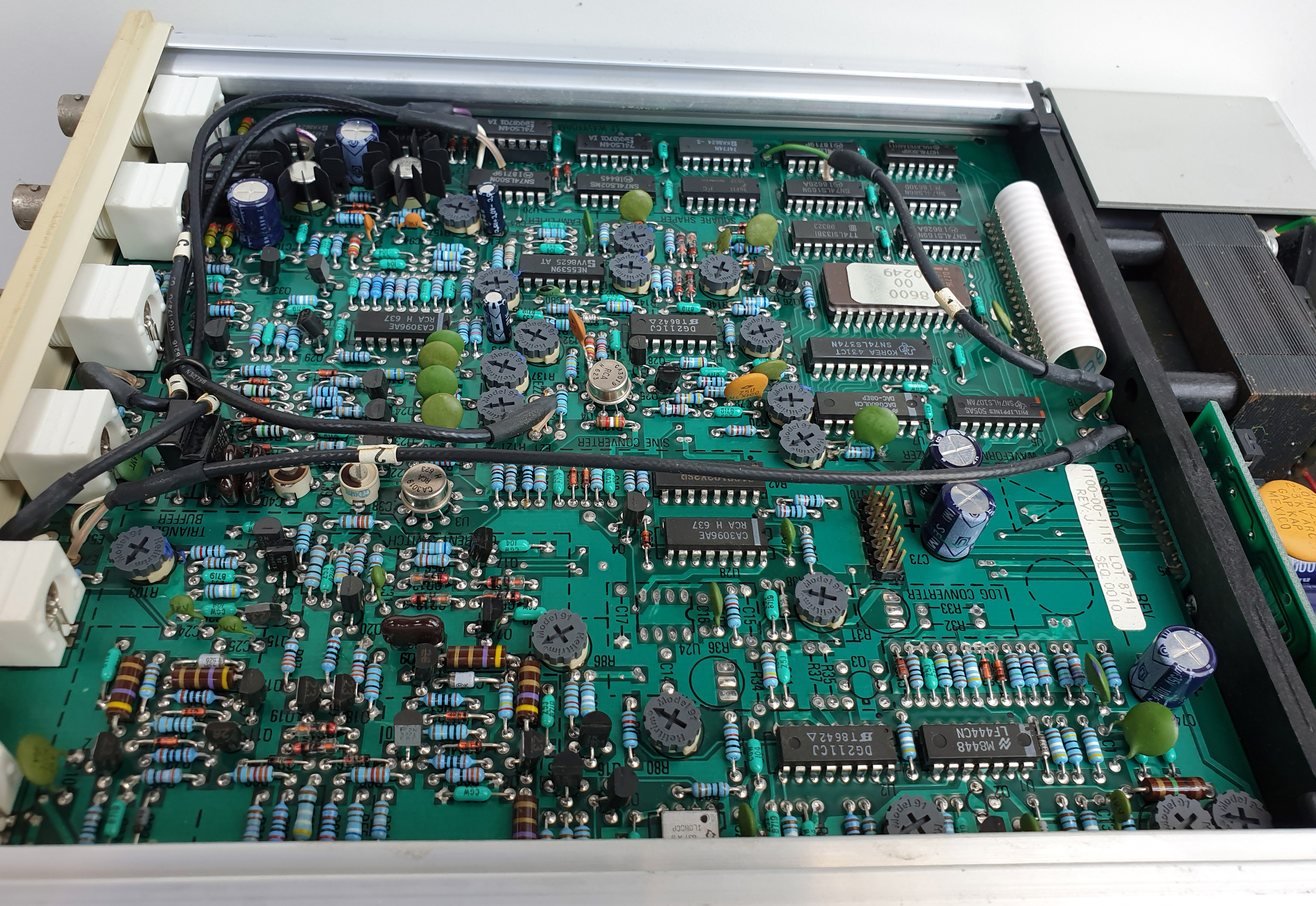
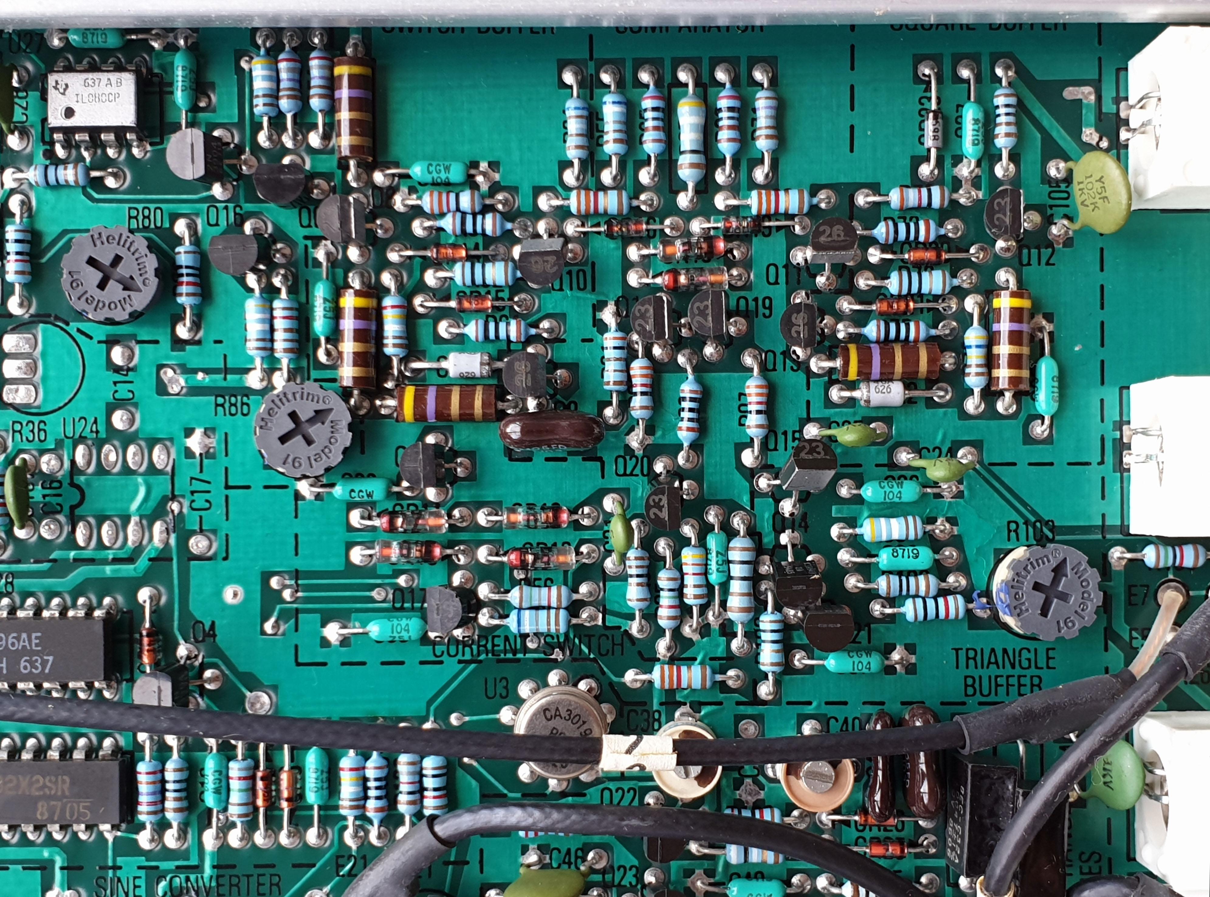
I think there should be ample clues in the first picture to guess the ware, but I included a couple of close-ups of the circuits because I love it when circuit boards document their functions so clearly. You can basically read the schematic directly off the traces. I also enjoy the motif of “here’s a ROM but no microprocessor” (the ROM is the ceramic-packaged 2716 in the top right of the first photo, with the label covering the UV erase window). ROM-based sequencers/FSMs and lookup tables were fairly common for this vintage, but these days most designs use ROMs exclusively to store code that is accessed by a CPU.
Andrew Huang's Blog

- Andrew Huang's profile
- 32 followers

