
Andrew Huang's Blog, page 42
May 17, 2013
Formlabs Form 1 Teardown
I got a Form 1 3D printer!
It’s the first 3D printer I’ve purchased (technically, I “backed” it). I managed to acquire a pre-release beta unit, as I’m affiliated with Neoteny Labs, one of Formlabs’ investors.
What’s the first thing I do with any shiny new gadget? That’s right, I take it apart!
Unboxing
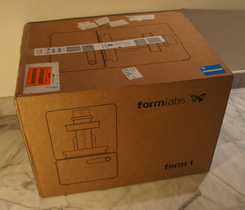
The complete Form 1 kit consists of three boxes: the printer (shown above), bottles of liquid photocurable resin, and a cleaning station. Many optical stereolithography printers require a cleaning step to wash off the uncured resin; for the Form 1 this means rinsing the part in isopropyl alcohol (the same stuff you use to disinfect cuts, but more concentrated) for a few minutes.
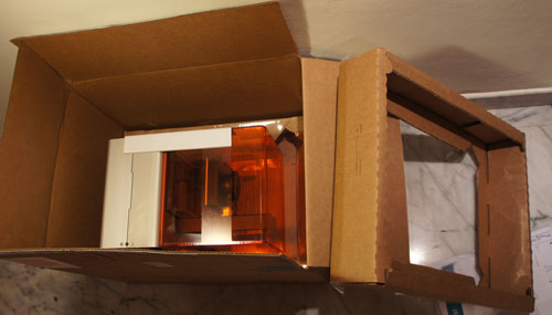
The packing method, at least for the beta, is styrofoam-free. It uses a pair of thin plastic sheets suspended on cardboard frames to hold the printer in a cradle. For a box that went as checked luggage from Boston to Singapore through three flights, it held up remarkably well.
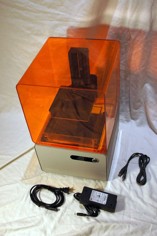
The printer box also contains the power supply, cables, and the requisite quickstart guides.
The serial number scheme, at least for the beta units, is “AdjectiveAnimalname”, so mine is simply “ChiefCat” — hurray for easy-to-read serial numbers!
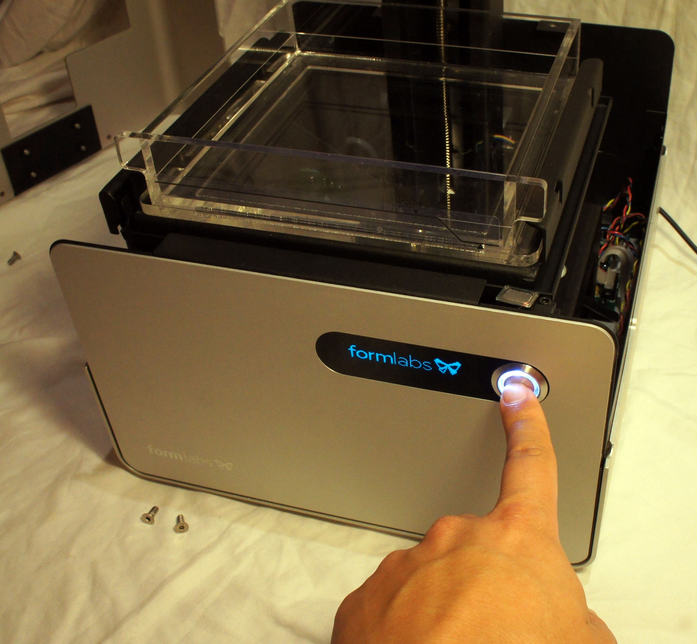
Undressing
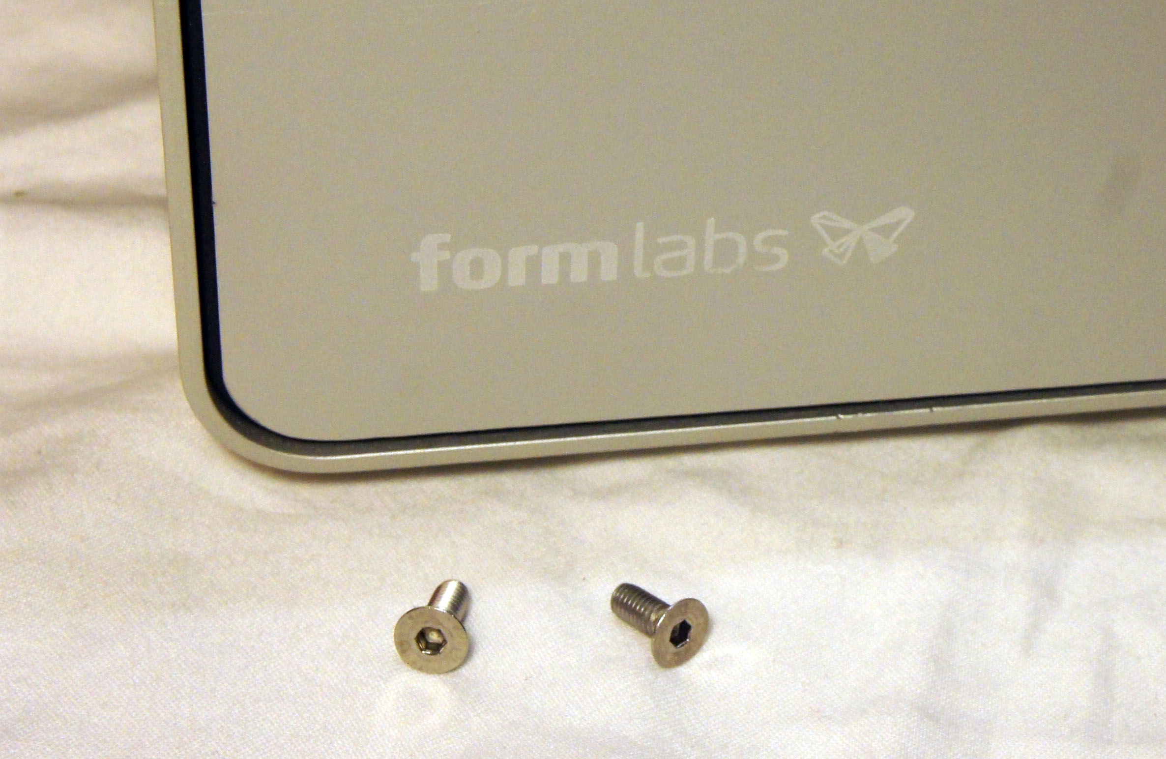
You need exactly one tool to disassemble the printer: a 2.5mm hex key (or, if you’re a fan of Torx, a T-10 bit). I really appreciate the balance of good design with practicality: it looks good, and you don’t need whacky pentalobe screwdrivers to service it. It does take a bit of elbow grease to undo the screws; but a grippy Torx driver makes short work of the problem without a single stripped screw.
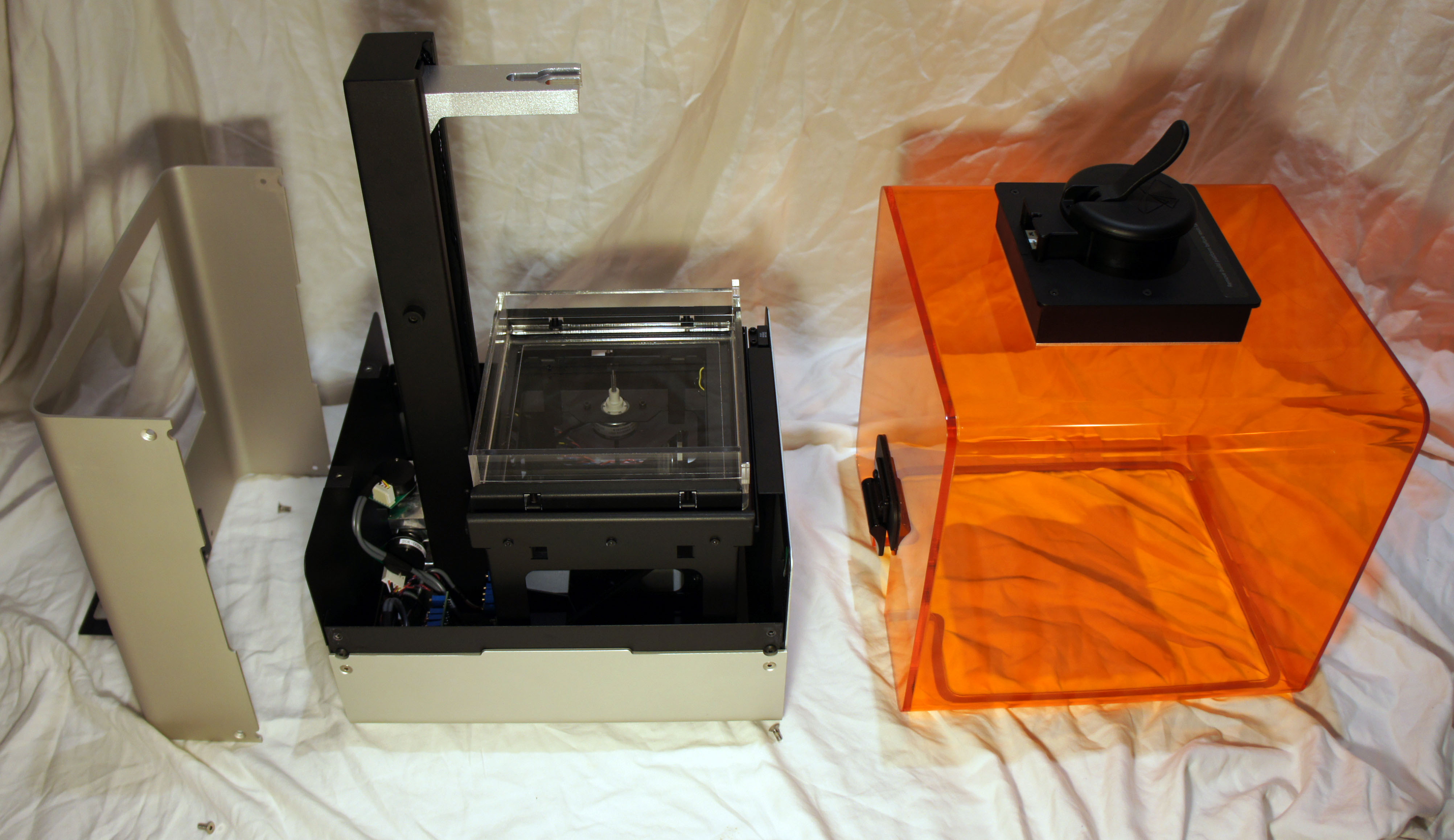
Two screws release the orange-colored light shield from its hinge, and four screws release the top of the base unit from the frame. The orange-colored shield protects your eyes from stray blue laser light, while also protecting the photosensitive resin bath on the inside from stray ambient light.

Six more screws (two of which are on the bottom) release the mid-frame from the base. The mid-frame is screwed to the front and back panels, but I didn’t need to remove the panels, as there is enough flexability in the sheet aluminum to slide the mid-frame off. The wiring to the front panel is tidily secured and is exactly the right length to allow the frame to sit next to the base without having to undo any cables — super-convenient for service and debug.
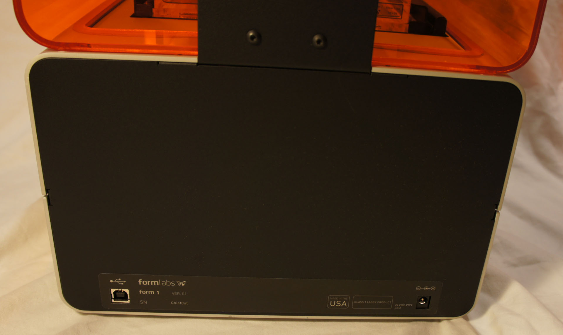
The inside of the front panel reveals the adapter for the OLED display, as well as the very handsome back-lit power button.
The Mechanism
One of the great things about a stereolithography 3D printer is that it uses a laser to cure a resin, instead of melting and extruding a plastic. As a result, the operation is whisper-quiet, and there is no odor during operation — you can put the printer in a bedroom and still sleep at night. To borrow the words of Obi-Wan Kenobi: “This is the 3D printer of a Jedi Knight. Not as clumsy or as random as an FDM, but an elegant tool for a more civilized age.”
I count four motors in the Form 1: two stepper motors with lead screws, and two galvonometers (which I refer to as simply “galvos”). Let’s tour the printer’s mechanisms, motor by motor.
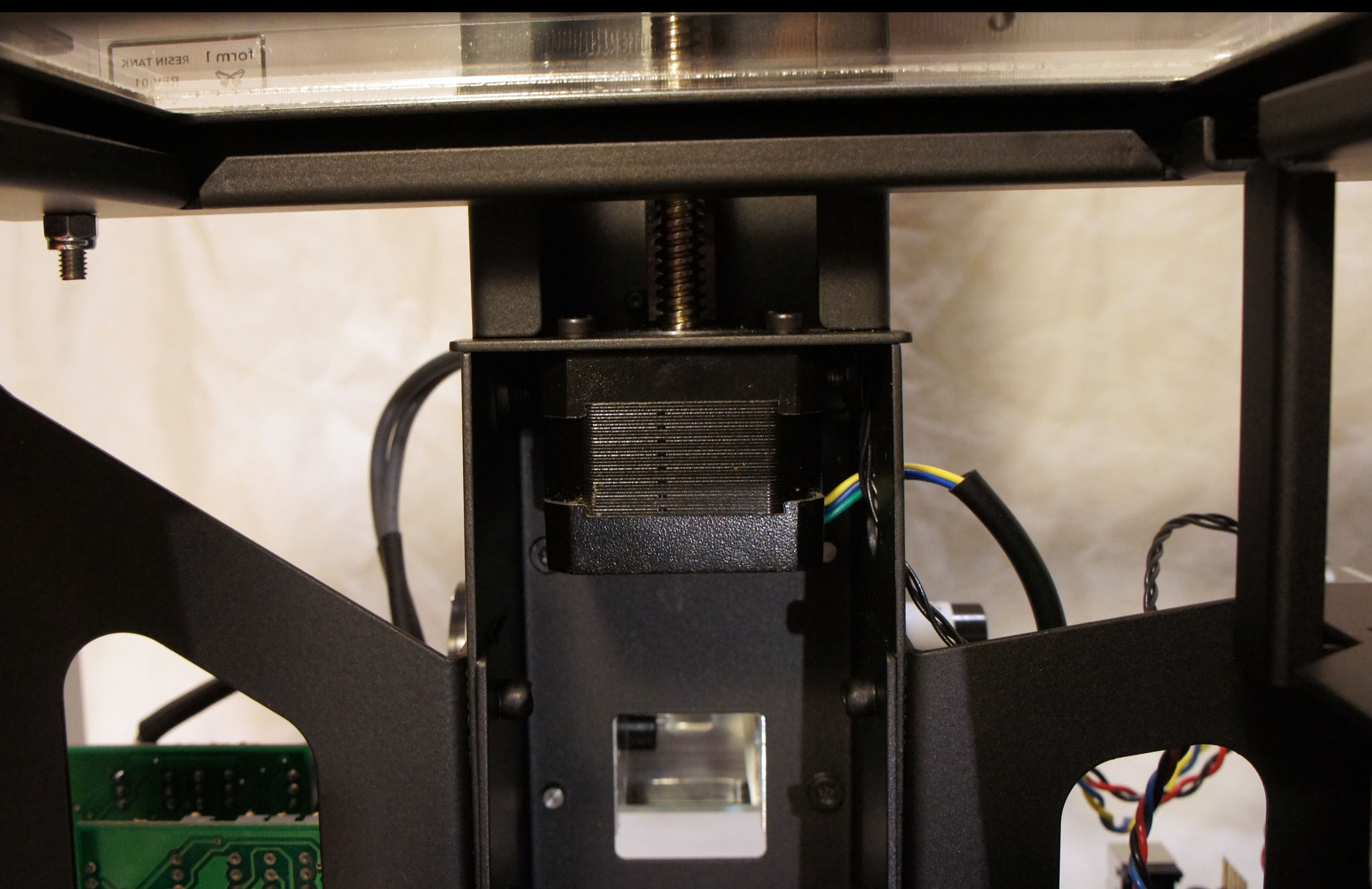
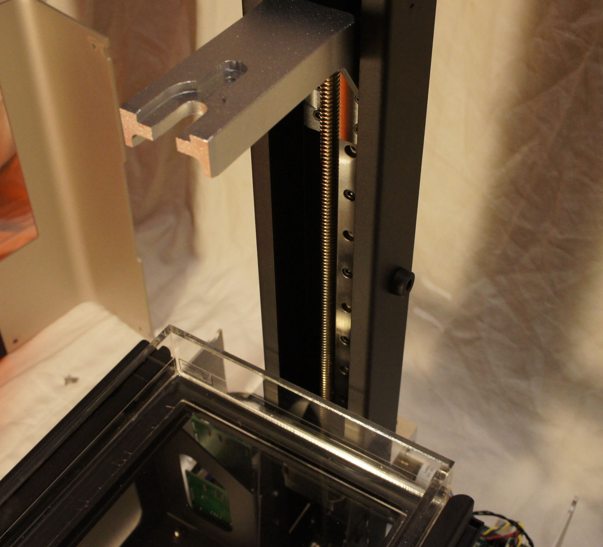
A large stepper motor with a lead screw running up the spine of the device pulls the build platform upwards. This causes the printed object to appear to “grow” out of the resin bath.
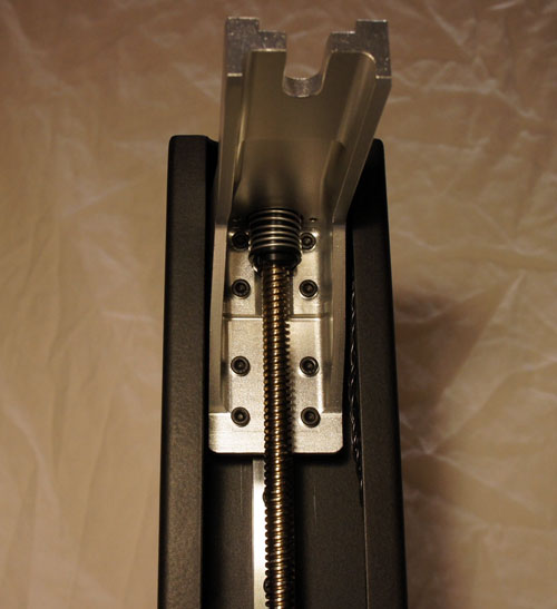
The build platform is attached to the leadscrew with an anti-backlash nut. The spring in the picture above applies a static force to the leadscrew-nut interface, reducing the play between the two and improving accuracy.

Every time a thin layer of resin is cured, a second motor performs a “peel” operation by tilting one edge of the resin tank downwards. The peel operation separates the newly formed layer from the bottom of the resin tank, allowing the build platform to move up freely. The leadscrew pictured above is responsible for this action, and it is driven by the smaller of two motors inside the Form 1. The white bearing is fixed to the frame, and the pin connecting the leadscrew to the tiltable resin tank is visible at the top.
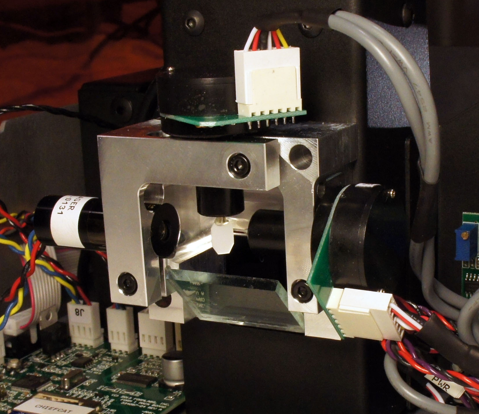
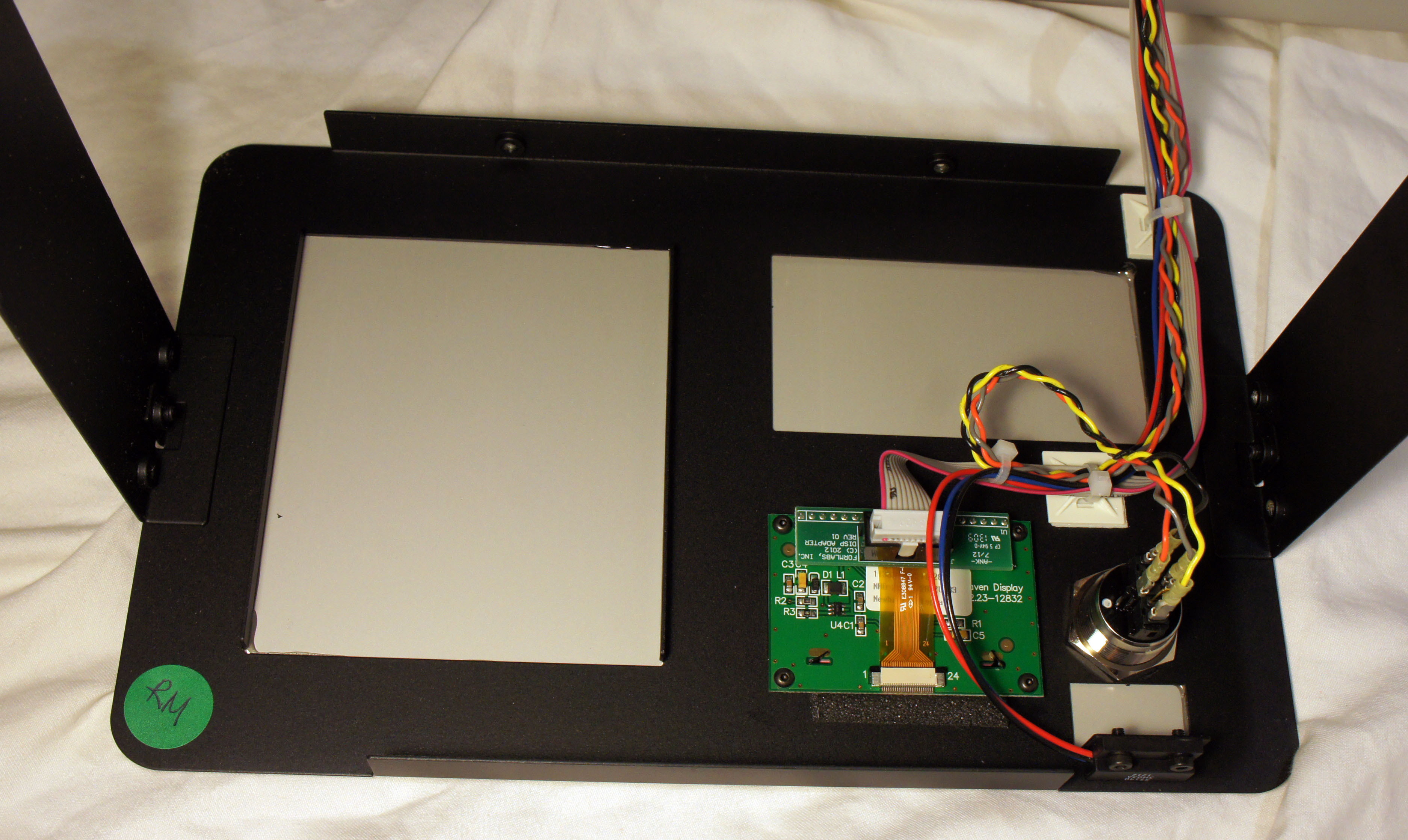
Ah…and now we peer into the heart of the Form 1! Here are the two remaining motors of the Form 1, the galvos. Galvos are very precise rotational actuators, with a built-in optical feedback loop (take a look inside one). The galvos each have a tiny octagonal mirror attached to their shafts, and are mounted at right angles to each other. One galvo steers the laser beam, entering from the left, along the X axis; then the light bounces to a second galvo that steers along the Y axis. The two working together can thus trace the 2-D vector pattern used to cure a single layer of resin. Below the galvos and laser is a mirror that reflects the light to another, larger mirror that finally shines the beam upwards into the resin bath.
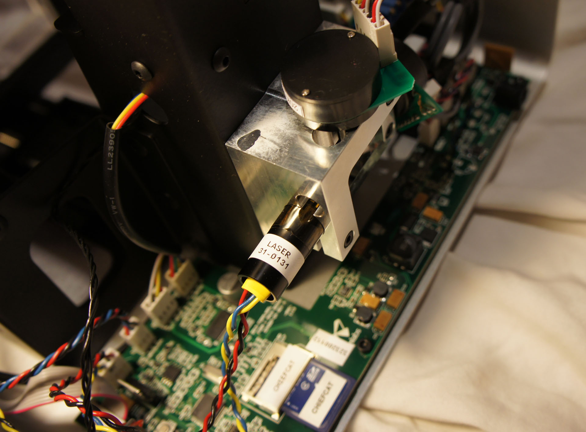
Above is another view of the laser. According to the safety warning bundled with the printer, it is a 405nm, 120mW violet laser diode (take a look inside one).
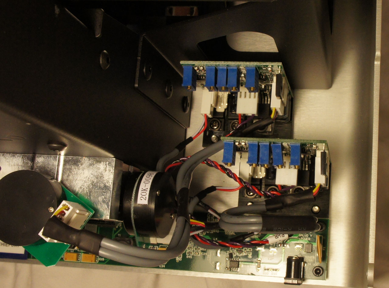
In order to achieve high performance, the galvo has a sturdy bank of drivers, mounted to the bottom aluminum surface of the case for heat sinking.
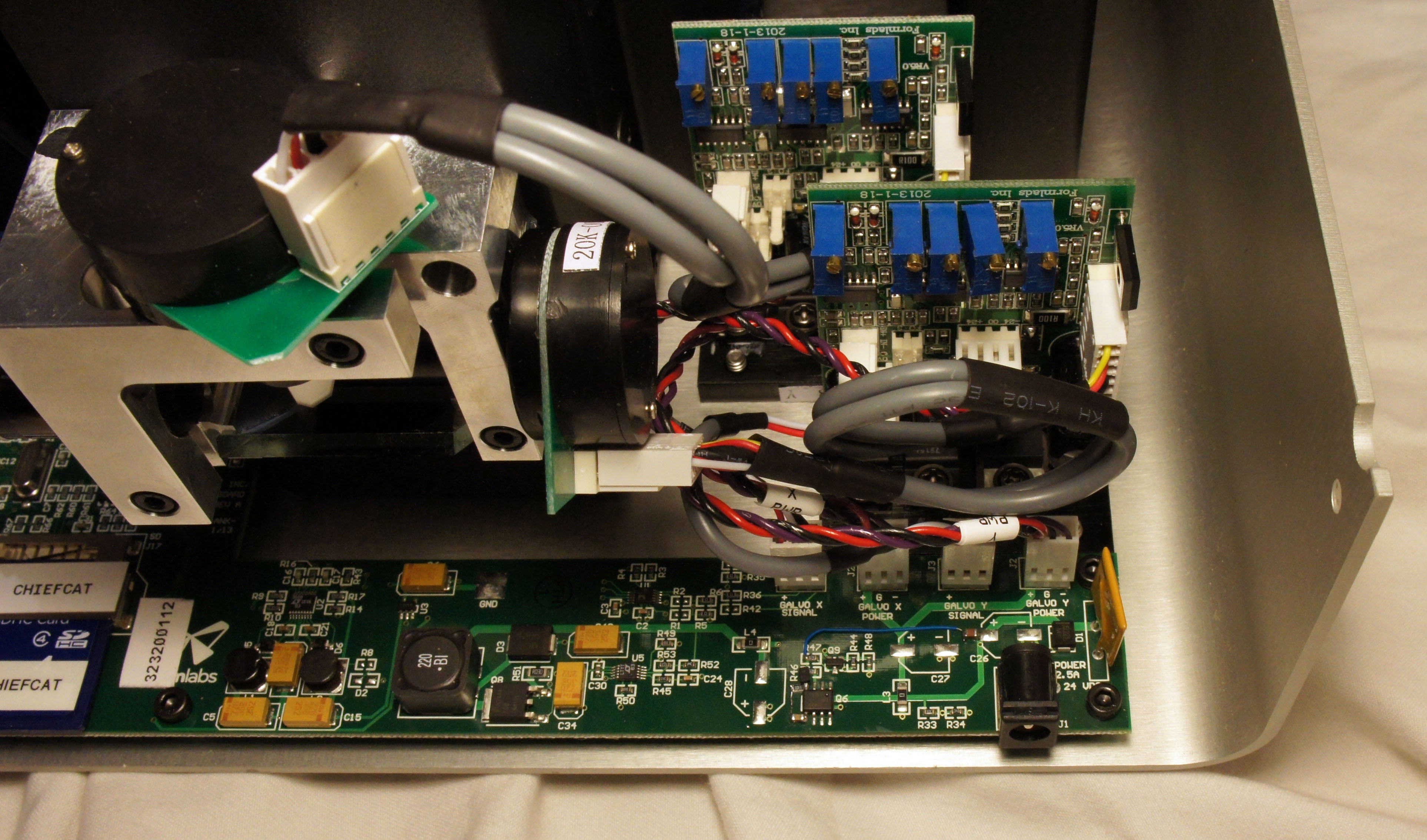
A slightly different camera angle shows the power input stage of the Form 1.
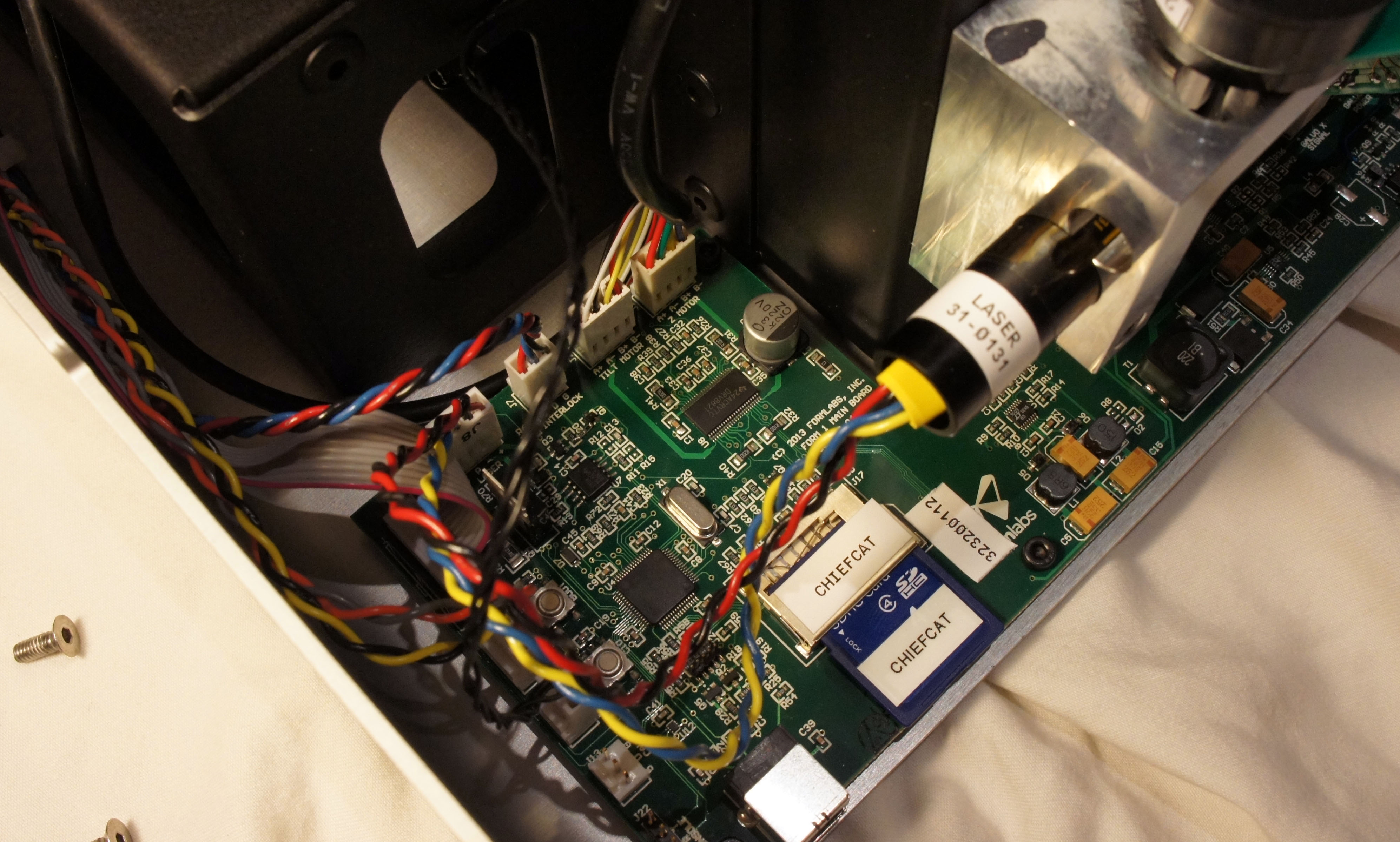
The main board wraps around the spine of the Form 1 and on the left side are the brains. An STM32 32-bit ARM Cortex-M3 microcontroller coordinates all of the activities inside the Form 1, and it appears that firmware for the device is stored on an internal, captive SD card.
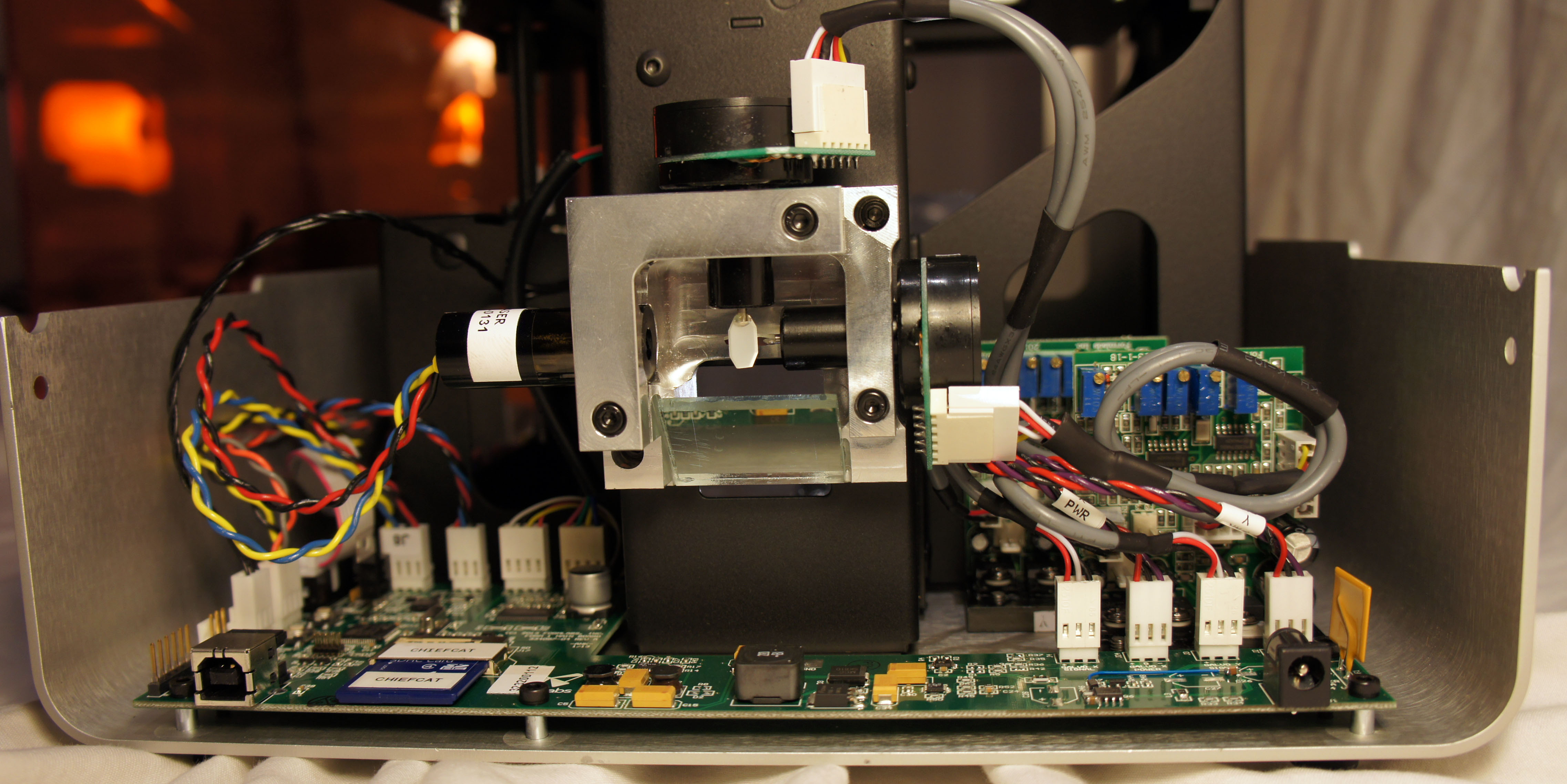

Above are some photos that give the whole context of the electronics behind the Form 1.
A hall effect sensor inside the base makes sure you can’t turn the device on when the protective light shield is lifted. But, you can defeat the sensor by putting a magnet on it, as I did above to check I hadn’t damaged anything before putting the whole thing back together again.
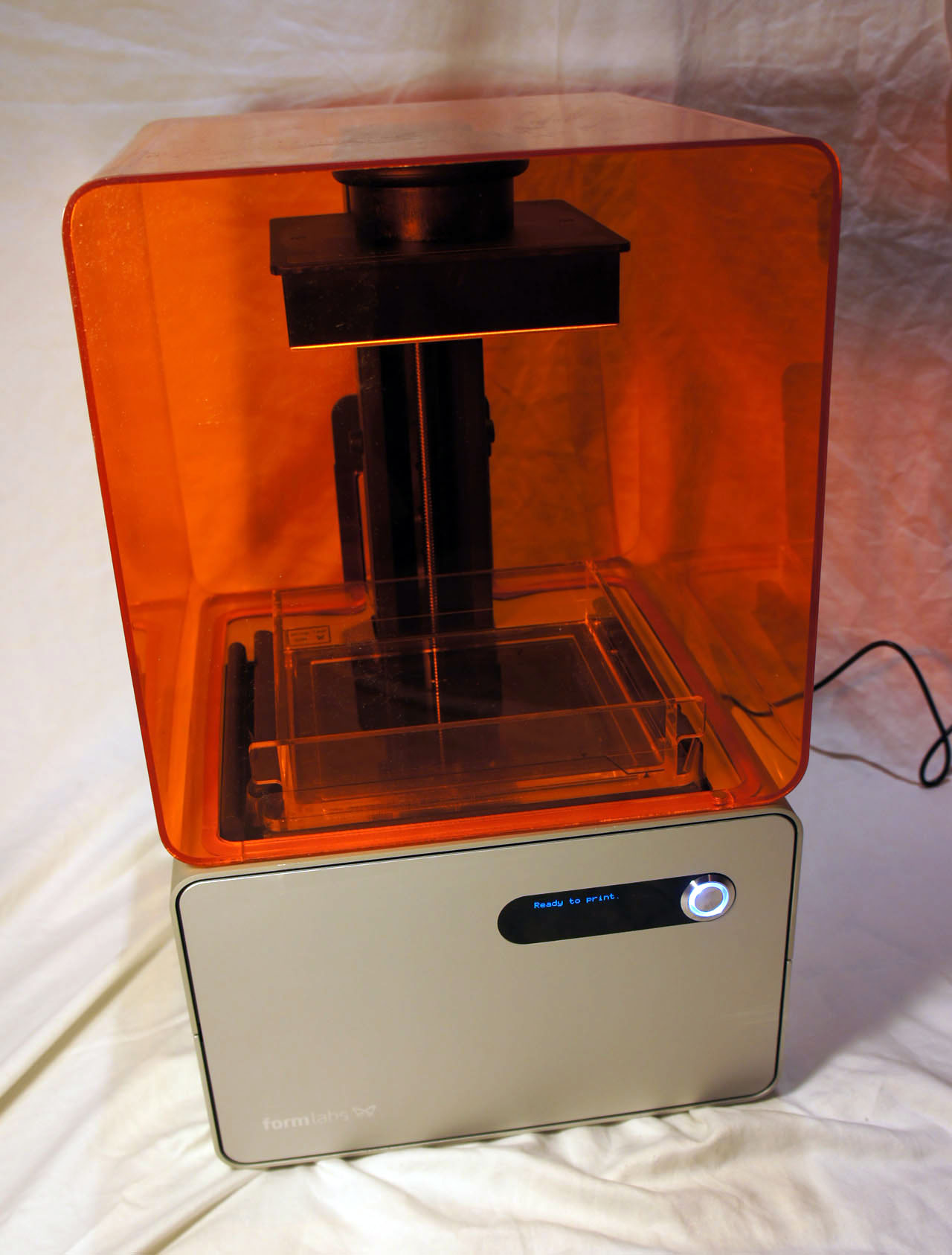
Re-assembly is a breeze — within a couple minutes I have the whole printer put back together and ready to do my first test print.
My First Print
What’s the first thing I’m going to print? I’m going to download and print a stand, designed by another user (IHeartEngineering) and shared for free, for my Geiger counter!
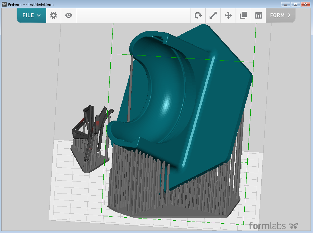
The Form 1 comes with a print management software package called “Preform”. It’s intuitive and easy to use; it allows you to place multiple objects on the build platform, duplicate, scale, and rotate. There’s an auto-orient feature that suggests an optimal orientation for supports based upon a DFM analysis. The screencap above is the result of the software picking the build orientation and populating the build supports.
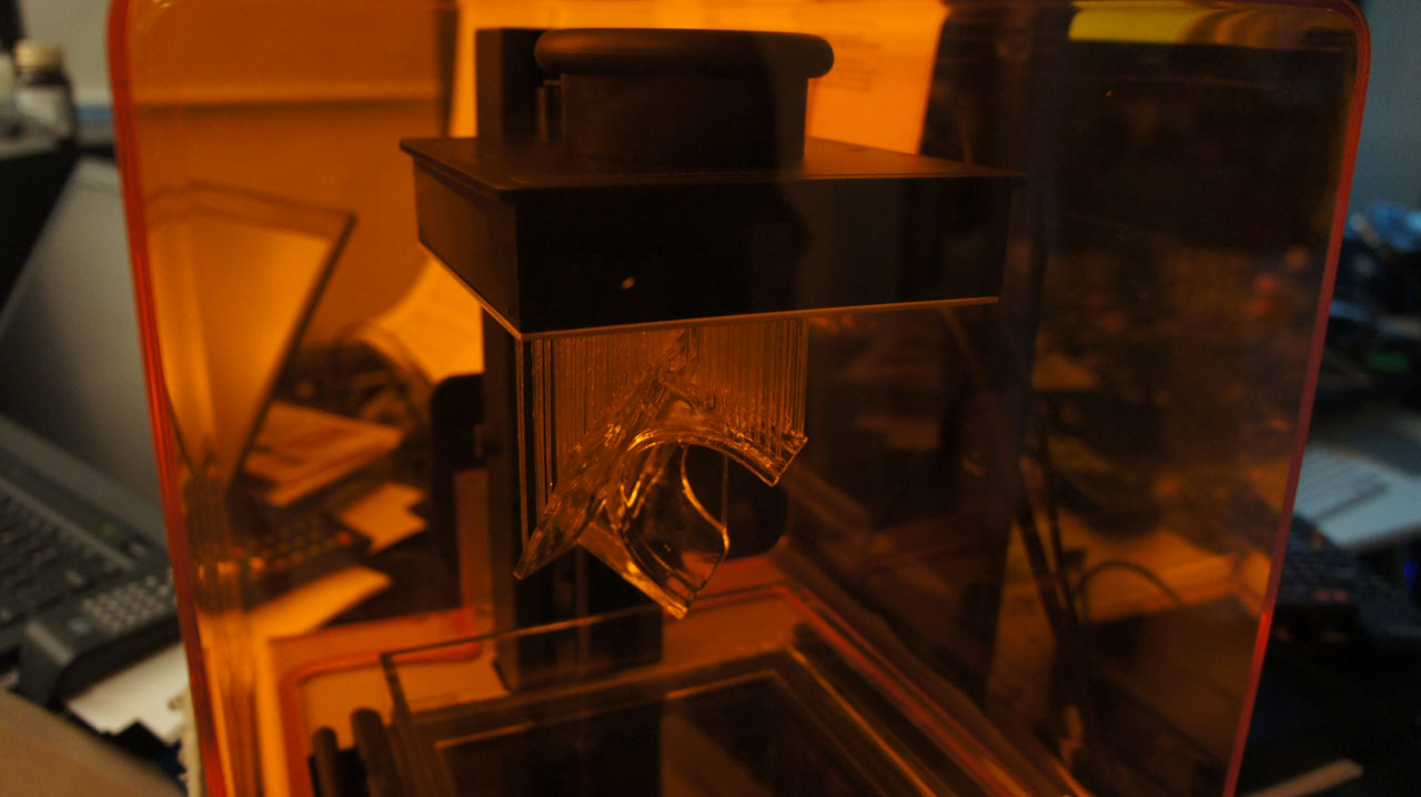
I click “Form”, and about 10 hours later the print is done.
The next step is to remove the build platform from the printer and bring it to the cleaning station, one of the accessories shipped with the Form 1. Cleaning is necessary to remove uncured liquid resin residue, and it’s recommended to handle uncleaned parts using gloves to avoid getting the goopy resin on your fingers.
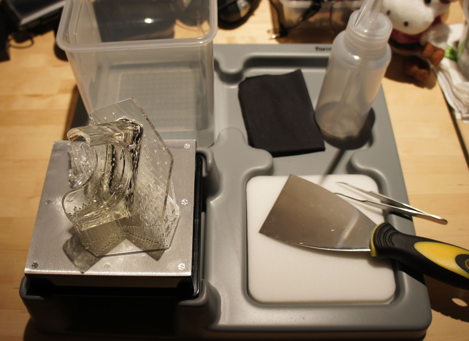
The cleaning station is thoughtfully laid out, with an area designed to hold the build platform. The kit includes some of the requisite tools to peel the part off of the platform, rinse it, and break off the supports. I supplement the kit with a pair of diagonal cutters for removing the supports, although you can also simply snap the supports off by pulling on them.
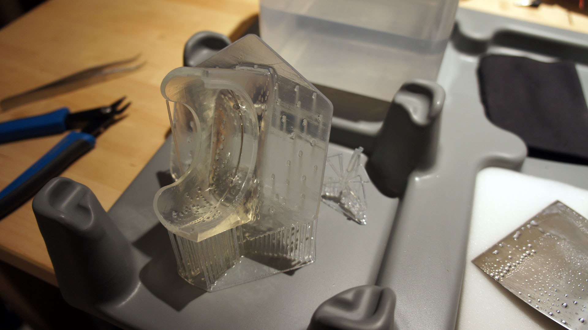
Two minutes of active shaking in an isopropyl bath, ten minutes of soaking, and the part is ready to be handled.
I use a pair of diagonal cutters to remove all of the supports in about five minutes.
This particular part features large, robust geometries: it’s designed to be printable on an FDM, so it doesn’t show off the high-resolution capability of the Form 1.
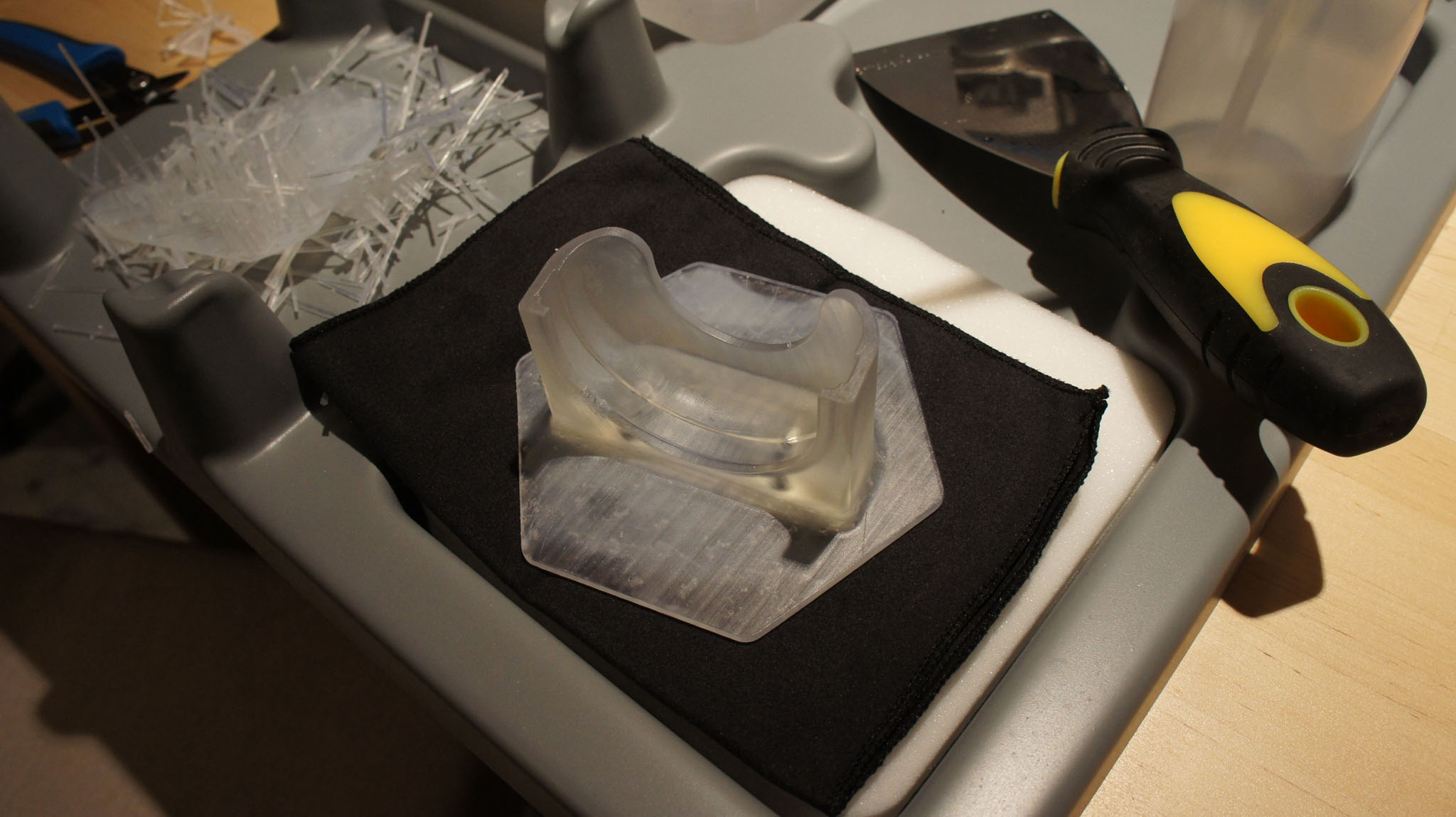
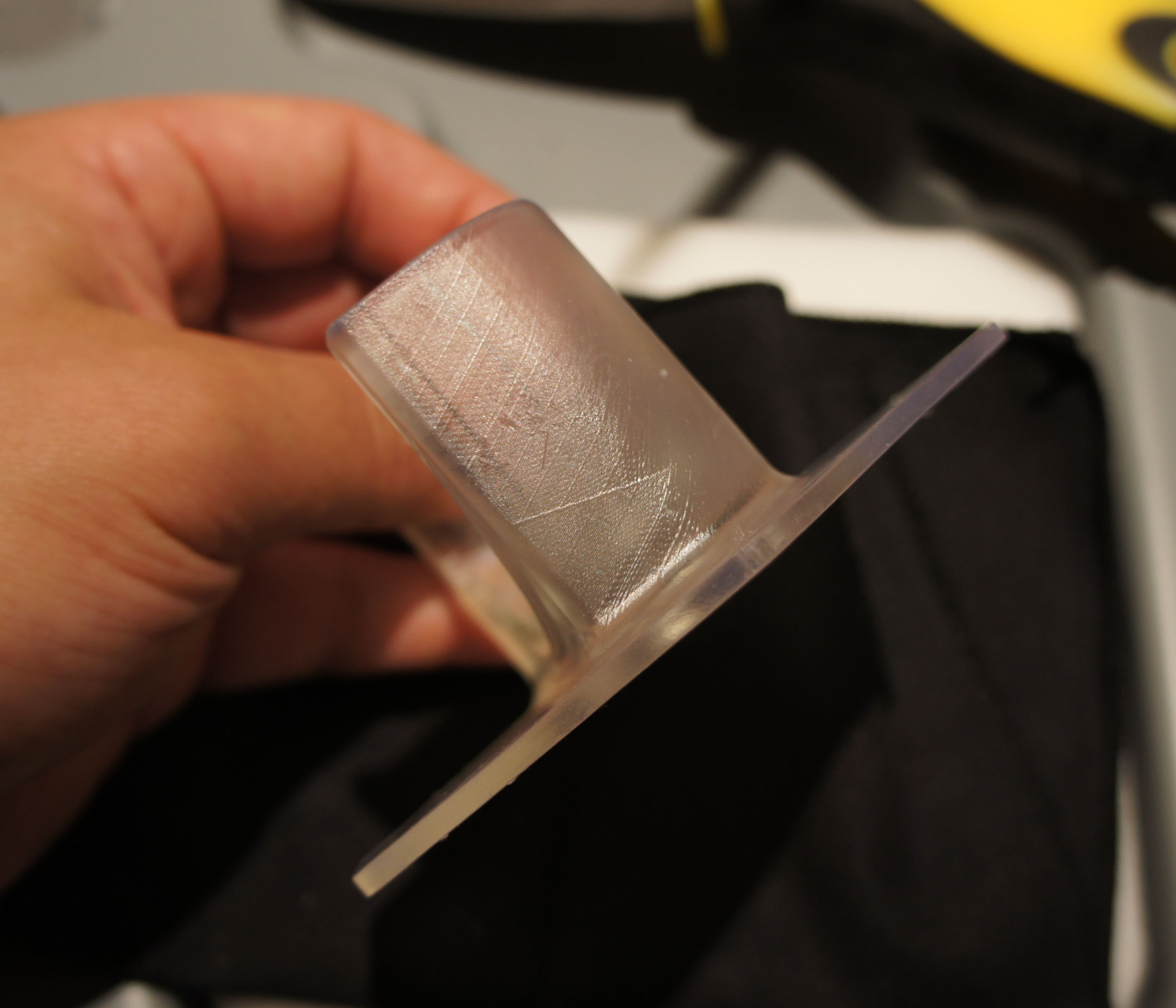
Small bumps are left on the area where the supports contact the part. These can be sanded off, if necessary.
The print is a success! It fits my Geiger counter like a glove.
And now for the shameless plug: if you made it all the way through this tear-down, and you’re a top-notch EE, you might want to consider applying for Formlabs’ Electrical Engineering Lead position by dropping them an email with your resume and cover letter.


May 10, 2013
Maker Faire and Hardware Innovation Workshop!
I’m looking forward to next week — one of my favorite events, Maker Faire, is just around the corner, and so is the Hardware Innovation Workshop.
I’ll be making the trek from Singapore this weekend so I can host a “Master Class Workshop” at the Hardware Innovation Workshop on the morning of May 14. Also in the line-up are Zach “Hoeken” Smith (haxlr8r), John Park (AQS), James “Laen” Neal (OSH Park PCB), and Zack Kaplan (Inventables), all of whom will share valuable insights and perspectives on manufacturing and scaling up.
We’ll be getting down to brass tacks with a group of Makers who are looking to scale their big ideas. We’ll share experiences about trying, and often times failing, to get things made. And we’ll finish with a set of campfire discussions, where Makers will get a chance to ask any questions weighing on their mind. If you liked my series of posts on “The Factory Floor”, you might also enjoy this workshop.
April 17, 2013
The $12 Gongkai Phone
How cheap can you make a phone?
Recently, I paid $12 at Mingtong Digital Mall for a complete phone, featuring quad-band GSM, Bluetooth, MP3 playback, and an OLED display plus keypad for the UI. Simple, but functional; nothing compared to a smartphone, but useful if you’re going out and worried about getting your primary phone wet or stolen.
Also, it would certainly find an appreciative audience in impoverished and developing nations.
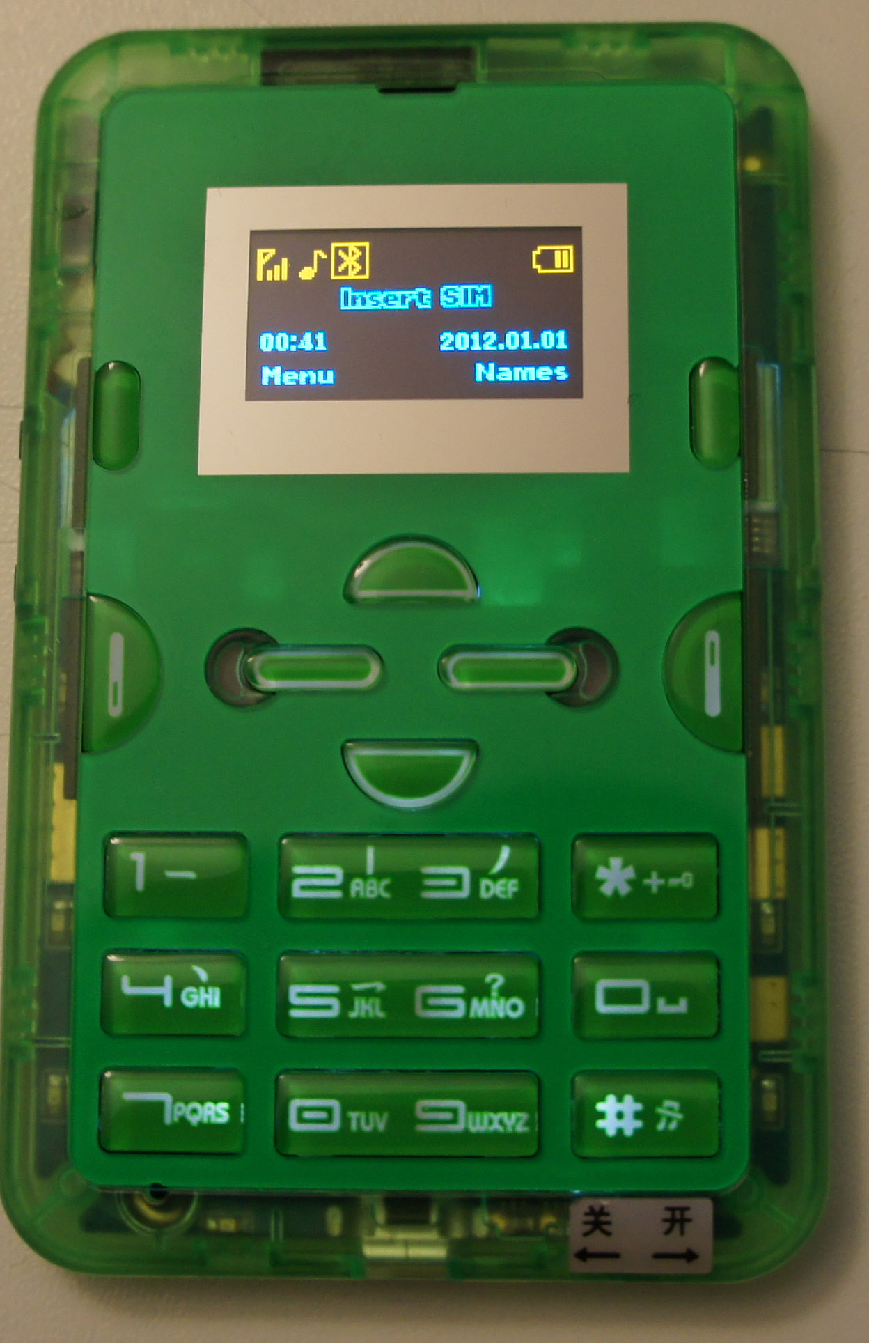
$12 is the price paid for a single quantity retail, contract-free, non-promotional, unlocked phone — in a box with charger, protective silicone sleeve, and cable. In other words, the production cost of this phone is somewhere below the retail price of $12. Rumors place it below $10.
This is a really amazing price point. That’s about the price of a large Domino’s cheese pizza, or a decent glass of wine in a restaurant. Or, compared to an Arduino Uno (admittedly a little unfair, but humor me):
Spec
This phone
Arduino Uno
Price
$12
$29
CPU speed
260 MHz, 32-bit
16 MHz, 8-bit
RAM
8MiB
2.5kiB
Interfaces
USB, microSD, SIM
USB
Wireless
Quadband GSM, Bluetooth
-
Power
Li-Poly battery, includes adapter
External, no adapter
Display
Two-color OLED
-
How is this possible? I don’t have the answers, but it’s something I’m trying to learn. A teardown yields a few hints.
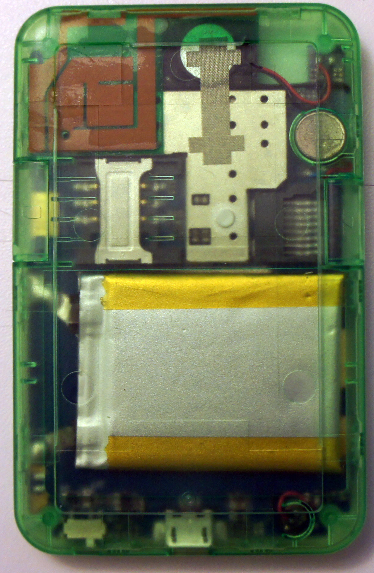
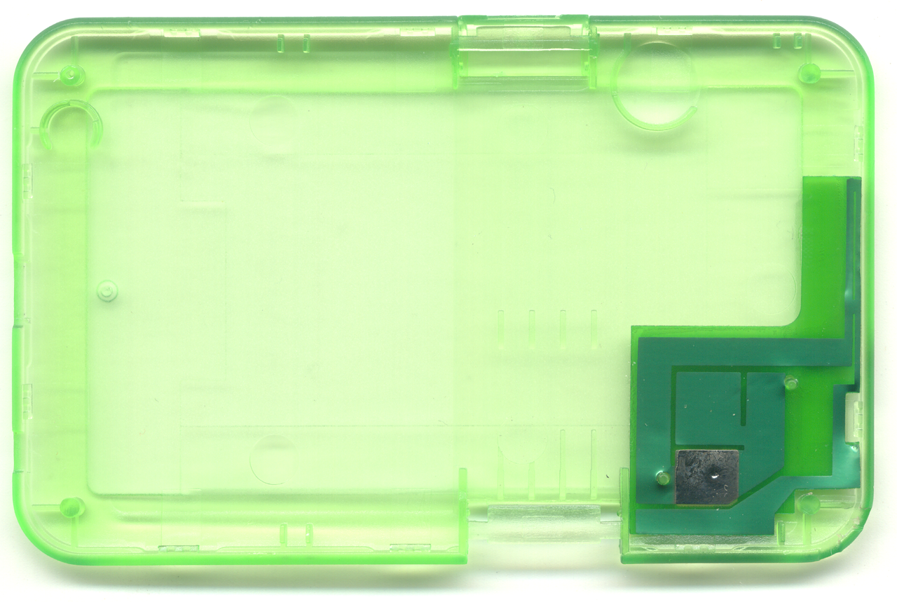
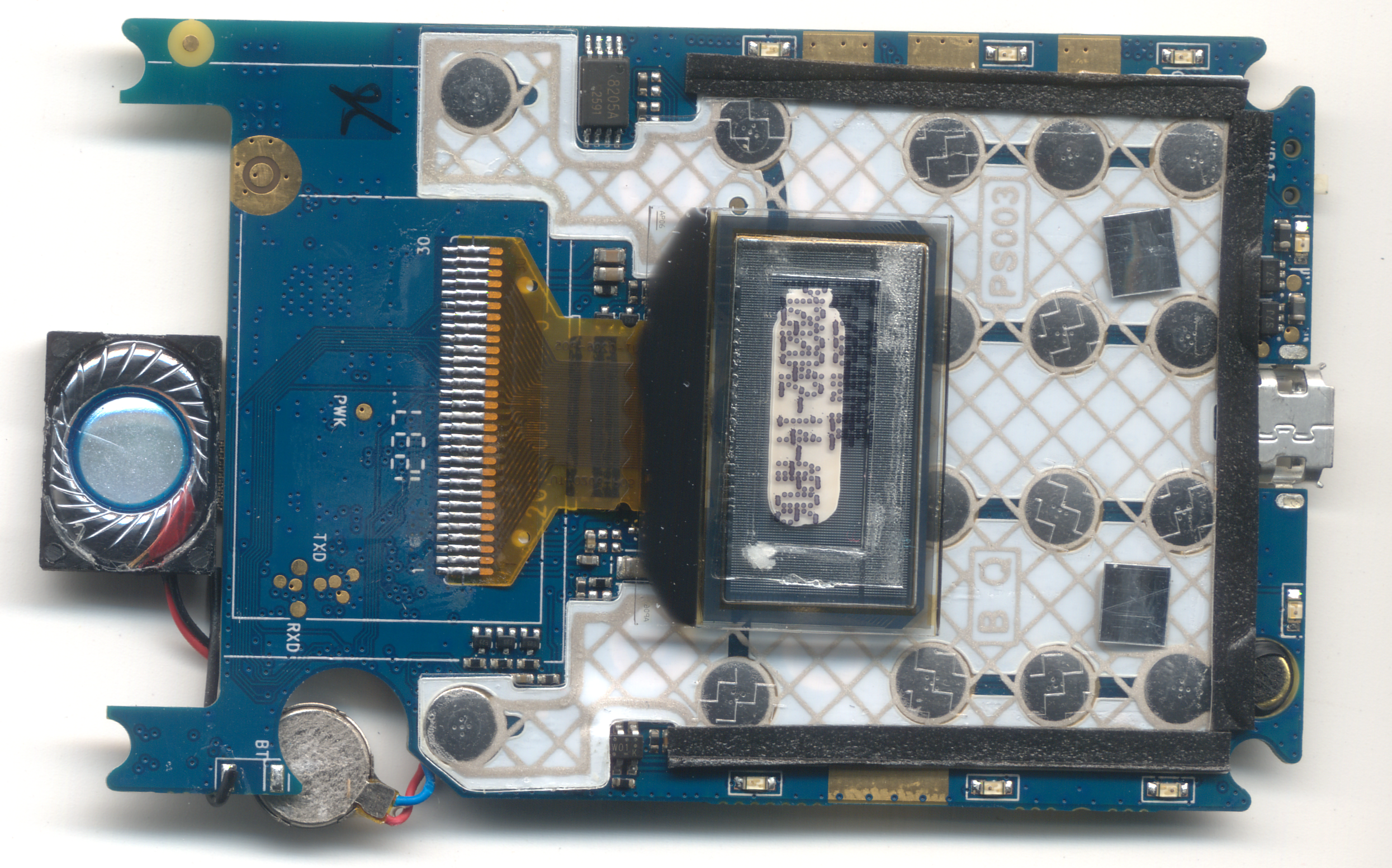
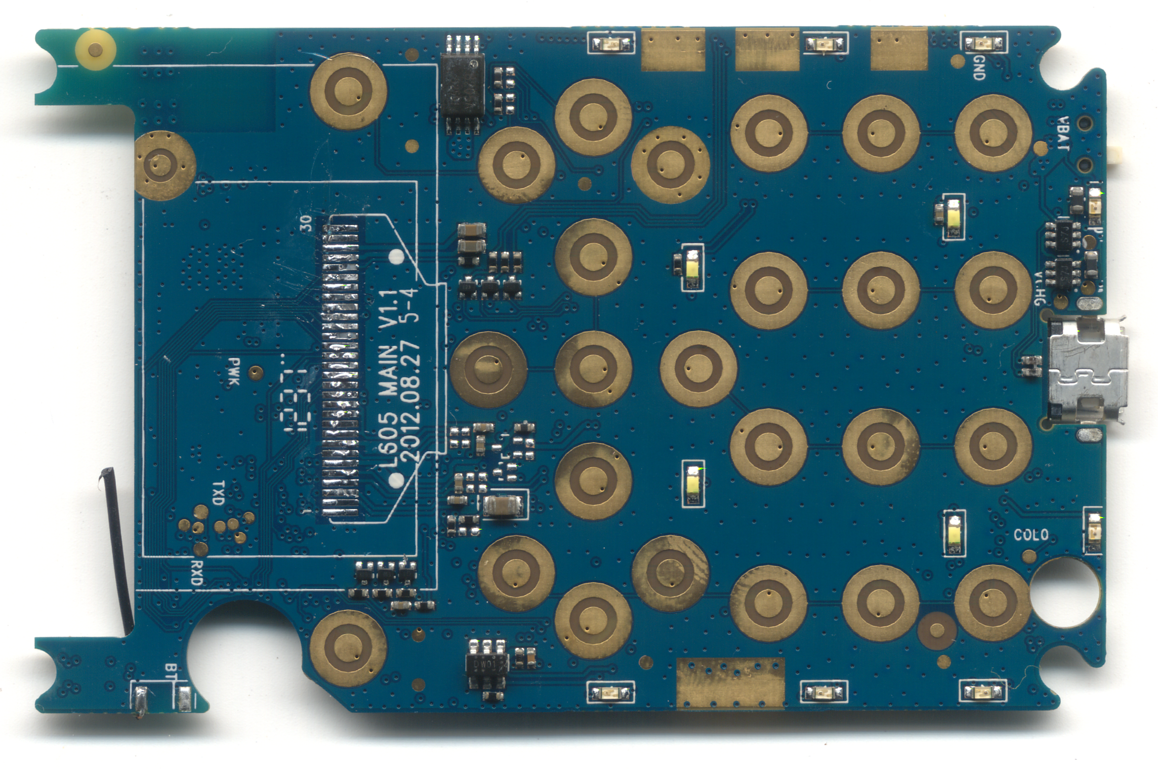
First, there are no screws. The whole case snaps together.
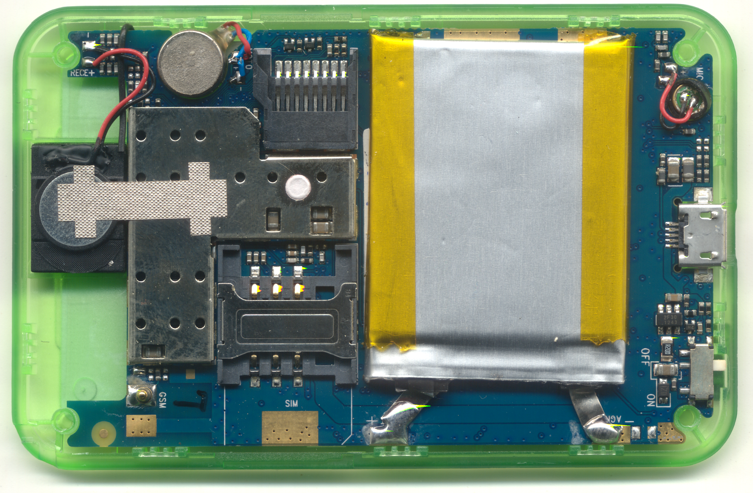
Also, there are (almost) no connectors on the inside. Everything from the display to the battery is soldered directly to the board; for shipping and storage, you get to flip a switch to hard-disconnect the battery. And, as best as I can tell, the battery also has no secondary protection circuit.
The Bluetooth antenna is nothing more than a small length of wire, seen on the lower left below.
Still, the phone features accoutrements such as a back-lit keypad and decorative lights around the edge.
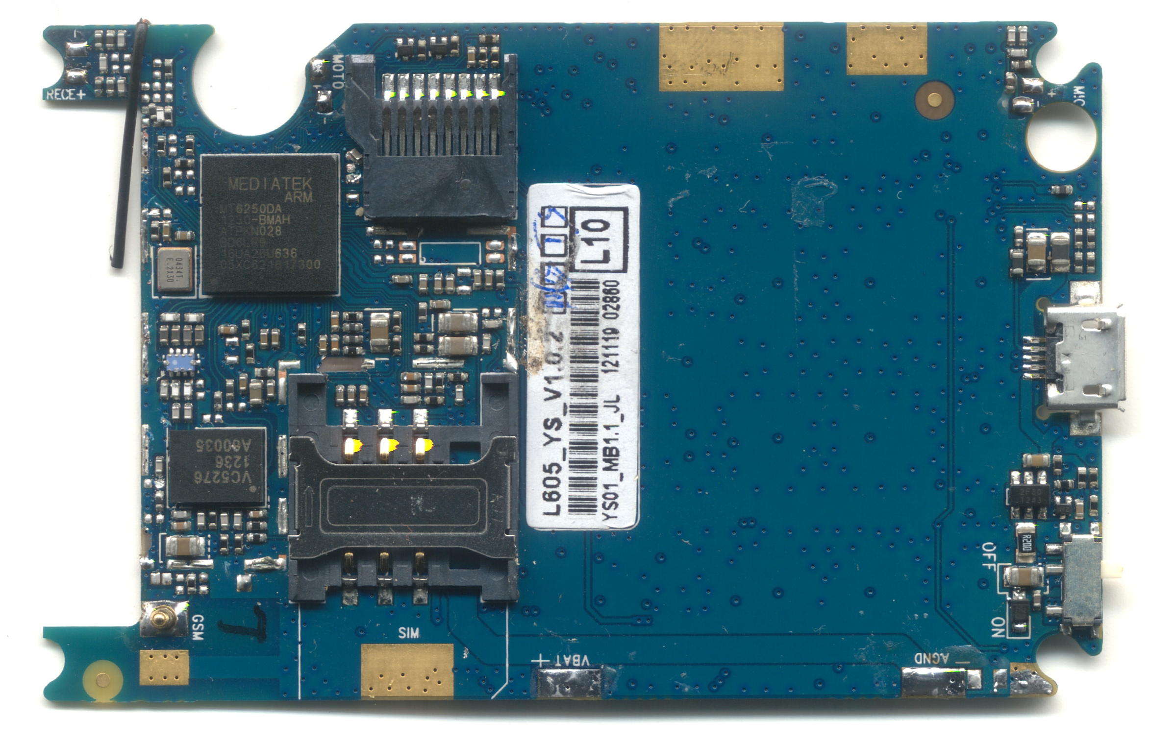
The electronics consists of just two major ICs: the Mediatek MT6250DA, and a Vanchip VC5276. Of course, with price competition like this, Western firms are suing to protect ground: Vanchip is in a bit of a legal tussle with RF Micro, and Mediatek has also been subject to a few lawsuits of its own.
The MT6250 is rumored to sell in volume for under $2. I was able to anecdotally confirm the price by buying a couple of pieces on cut-tape from a retail broker for about $2.10 each. [No, I will not broker these chips or this phone for you...]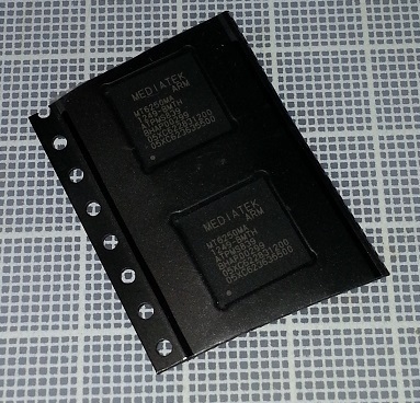
That beats the best price I’ve ever been able to get on an ATMega of the types used in an Arduino.
Of course, you can’t just call up Mediatek and buy these; and it’s extremely difficult to engage with them “going through the front door” to do a design. Don’t even bother; they won’t return your calls.
However, if you know a bit of Chinese, and know the right websites to go to, you can download schematics, board layouts, and software utilities for something rather similar to this phone…”for free”. I could, in theory, at this point attempt to build a version of this phone for myself, with minimal cash investment. It feels like open-source, but it’s not: it’s a different kind of open ecosystem.
Introducing Gongkai
Welcome to the Galapagos of Chinese “open” source. I call it “gongkai” (公开). Gongkai is the literal translation of “open” as applied to “open source”. I feel it deserves a term of its own, as the phenomenon has grown beyond the so-called “shanzhai” (山寨) and is becoming a self-sustaining innovation ecosystem of its own.
Just as the Galapagos Islands is a unique biological ecosystem evolved in the absence of continental species, gongkai is a unique innovation ecosystem evolved with little western influence, thanks to political, language, and cultural isolation.
Of course, just as the Galapagos was seeded by hardy species that found their way to the islands, gongkai was also seeded by hardy ideas that came from the west. These ideas fell on the fertile minds of the Pearl River delta, took root, and are evolving. Significantly, gongkai isn’t a totally lawless free-for-all. It’s a network of ideas, spread peer-to-peer, with certain rules to enforce sharing and to prevent leeching. It’s very different from Western IP concepts, but I’m trying to have an open mind about it.
I’m curious to study this new gongkai ecosystem. For sure, there will be critics who adhere to the tenants of Western IP law that will summarily reject the notion of alternate systems that can nourish innovation and entrepreneurship. On the other hand, it’s these tenants that lock open hardware into technology several generations old, as we wait for patents to expire and NDAs to lift before gaining access to the latest greatest technology. After all, 20 years is an eternity in high tech.
I hope there will be a few open-minded individuals who can accept an exploration of the gongkai Galapagos. Perhaps someday we can understand — and maybe even learn from — the ecosystem that produced the miracle of the $12 gongkai phone.
April 14, 2013
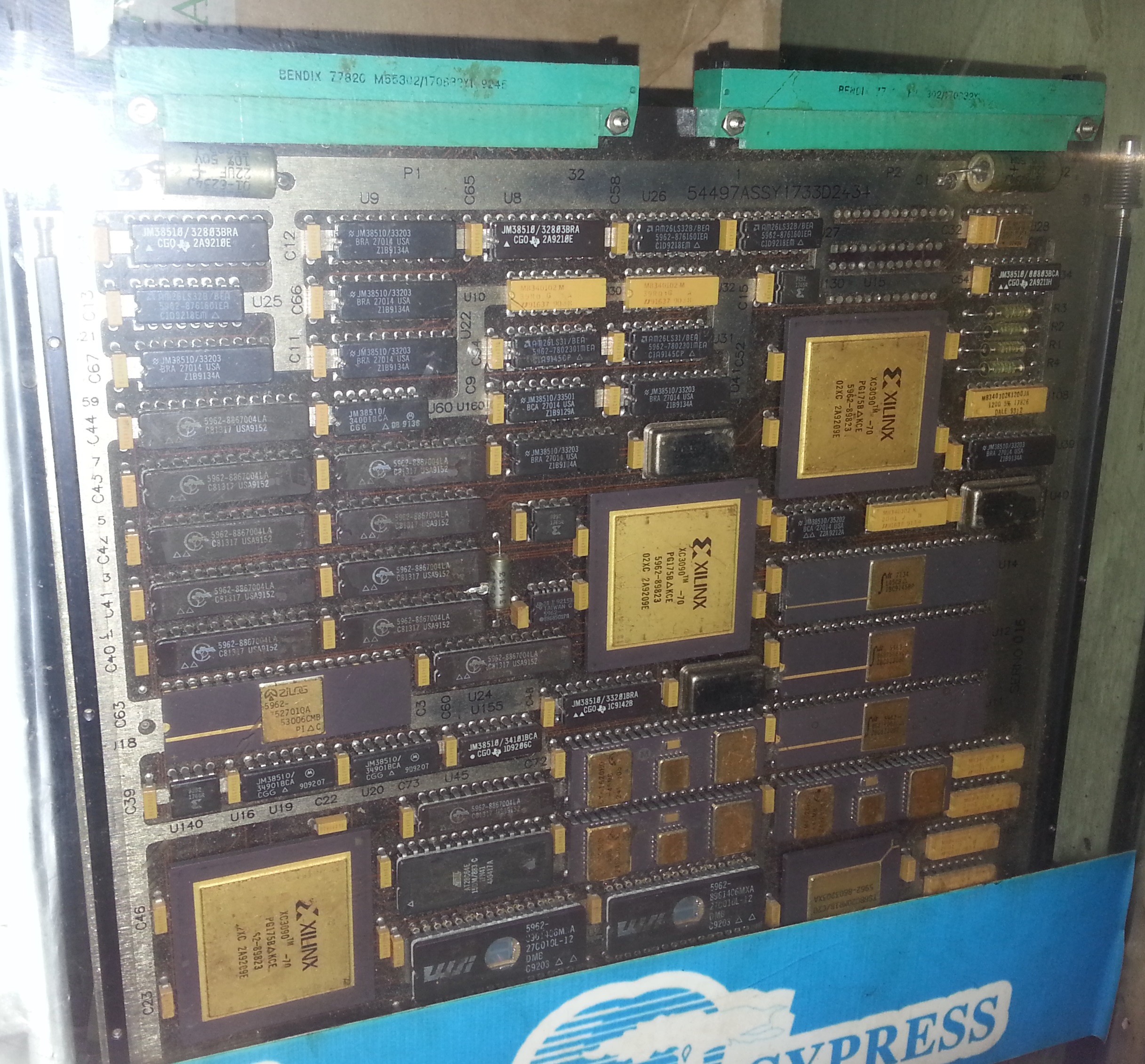
Name that Ware April 2013
The Ware for April 2013 is below. Click on the image for a larger version.

I found this board while wandering a dimly-lit, obscure corner of the Hua Qiang electronics district on a quiet Sunday. My apologies for the less than optimal photo quality, I only had my cell phone camera on me and I was trying to snap shots while being subtle about it.
I have no idea what this board does, but the mil-spec ratings on the parts immediately caught my eye; I’ve previously come across boards that were clearly from missiles and guidance systems in the markets, but I was unable to get a photo of them, as the vendor wouldn’t allow it.
Some alternate angles of the board are available here and here. Curious to see if anyone can positively identify the ware!
Winner, Name that Ware March 2013
The ware from March 2013 is a serial link card from a Kodak X-ray Medical Imaging Manager. As Julien was the first to identify it, he’s the winner, congrats and email me for your prize!
Sorry for the short synopsis of the ware, it’s been a busy month and I’m struggling to keep up…
March 11, 2013
Releasing free PDF of “Hacking the Xbox” in honor of Aaron Swartz
No Starch Press and I have decided to release a free ebook version of Hacking the Xbox in honor of Aaron Swartz. As you read my book, I hope that you’ll be reminded of how important freedom is to the hacking community and that you’ll be inclined to support the causes that Aaron believed in.

Apologies in advance if there are any hiccups in the distribution of the free copy. The file is being hosted from a server in my flat, which only has a 100Mbps up-link (currently pushing >30Mbps).
March 10, 2013
Open Source Geiger Counter Update
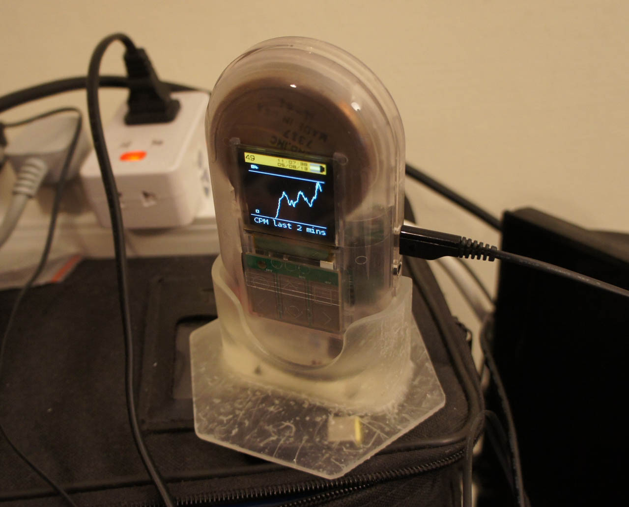
Today, March 11, marks the second anniversary of the Tohoku-Oki earthquake that devastated Japan and triggered the meltdown of Fukushima Daiichi. In a desire to help any way I could, I joined Safecast and created an open source Geiger counter reference design, which I released last year around this time.
Since then, Safecast launched a successful Kickstarter campaign, and International Medcom has completed the monumental tasks of tooling, testing, debugging, and developing firmware for this little device.
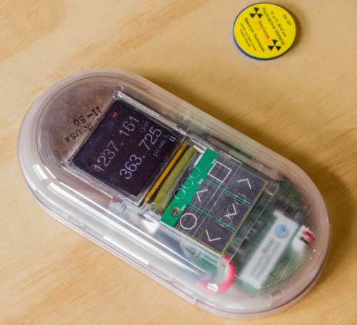
Above: the limited edition Kickstarter version of the Geiger counter in action.
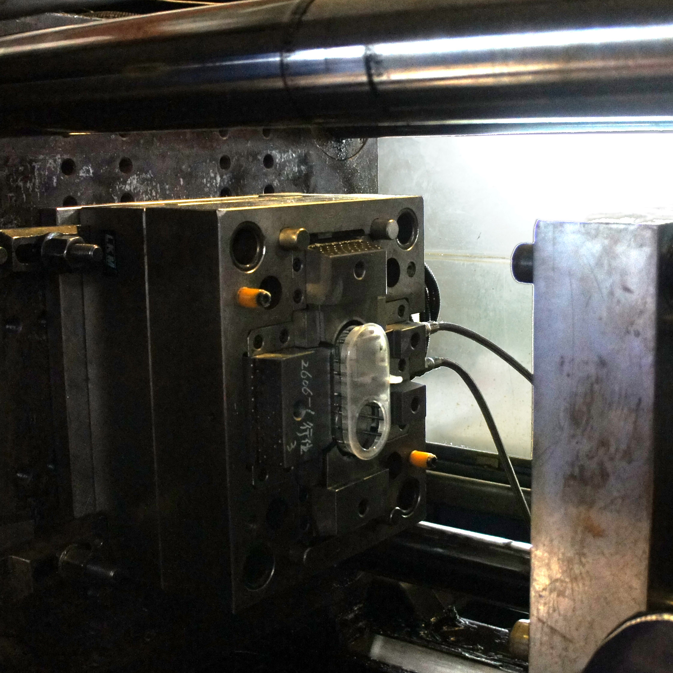
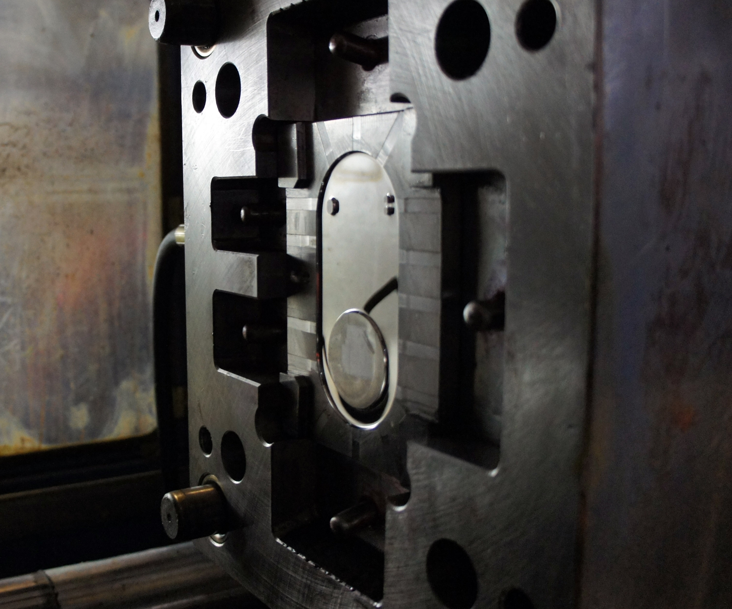
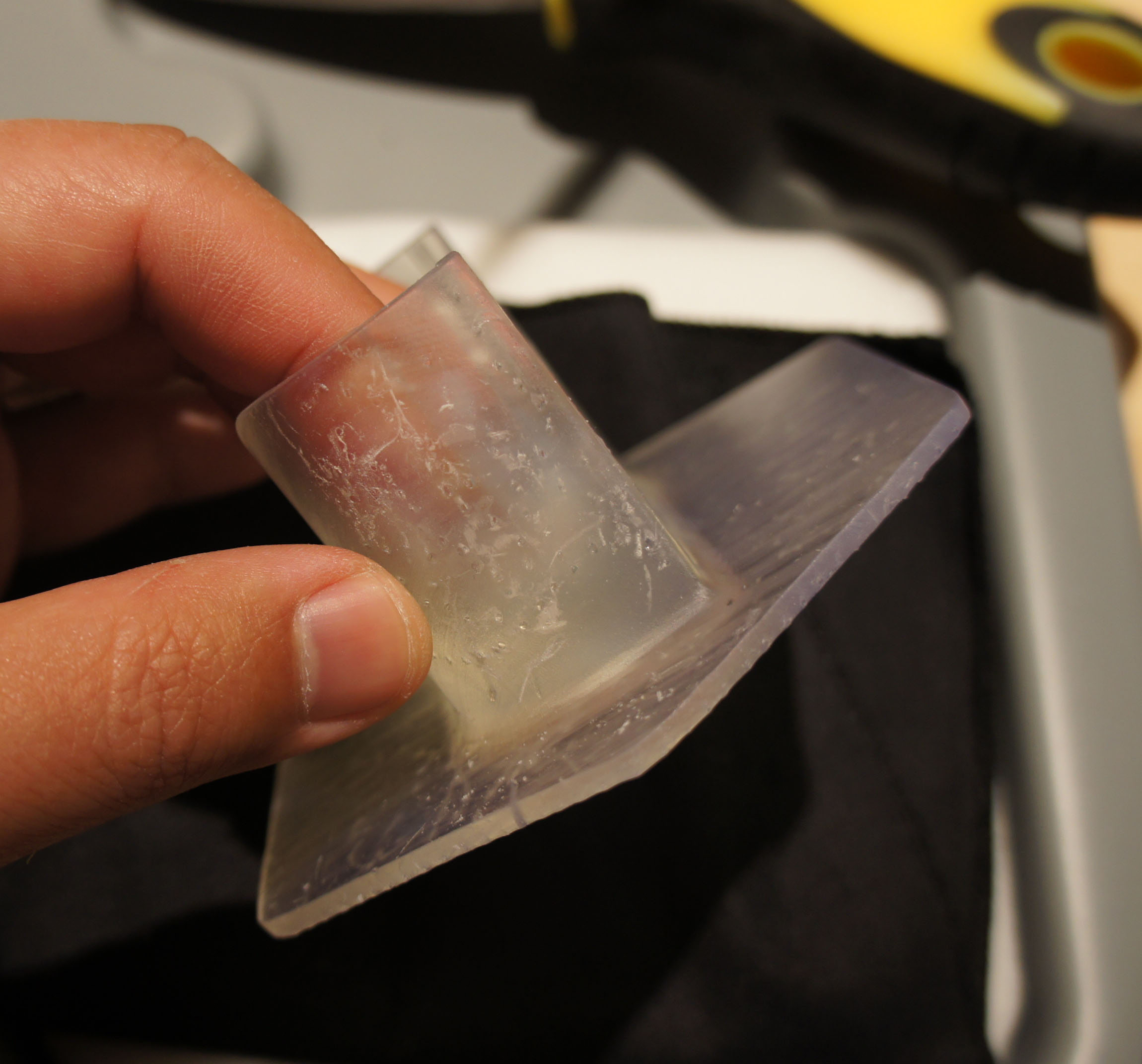
Above: the steel tools used to injection mold the ventral case of the Geiger counter.
Finally, the clear, limited-edition Kickstarter devices are shipping. You can see some photos of them on the Make Blog as Eric Weinhoffer at Make is helping to put the finishing touch on every unit: a laser-cut, limited edition serial number on the back of each case.
Having shipped many products myself, I know how hard everyone has worked to make this a reality. Congrats guys!
If you donate to Safecast between now and 11:59 PM EDT tomorrow, March 11th, Global Giving will match your donation 200%. As long as funding remains, they’ll even match your donation 100% until March 15th. Click the image below to learn more and contribute to a great project.
Name that Ware March 2013
The Ware for March 2013 is shown below. Click on the image for a larger version.
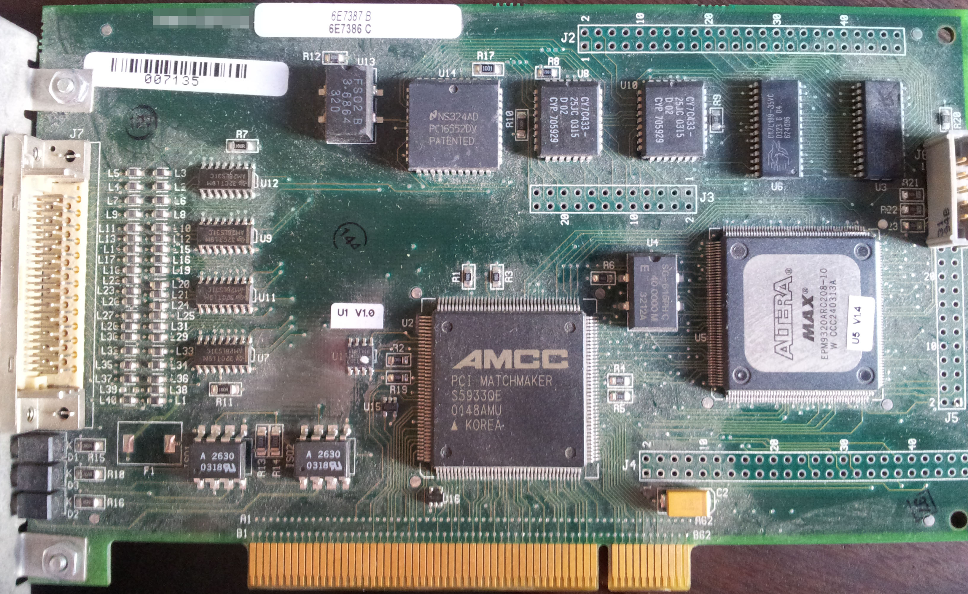
Thanks to Patricio Worthalter for contributing this month’s ware! The PCI Matchmaker from AMCC brings me back. I used one of those as part of my Master’s thesis, back in the day when FPGAs accessible by mere mortals couldn’t do PCI directly. Man, it was (and still is) a pain to properly obtain the official PCI bus specs…PCI is a member’s-only club, with a $3k annual fee. Ain’t nobody got dime fo’ that!
Winner, Name that Ware February 2013
The Ware for February 2013 is the Worldsemi WS2812. It’s a digital-to-light converter — add +5V, ground, and shift in a digital code word, and out comes PWM RGB light. The chip also features a digital output for cascading multiple LEDs in a row. It’s an extremely versatile chip that was brought to my attention by Dave Cranor during the Shenzhen geek tour in January — one of those things that you just keep a stock of at all times because it’s a dirt simple way to add a beautiful-looking LED into a tight spot. You can buy ones mounted on a little PCB from Adafruit.
I’ll give Randy the prize this month, since he was the first to correctly identify the entire packaged ware, and also gave a link to a datasheet (which I had also been looking for). Thanks, and email me for your prize!
February 11, 2013
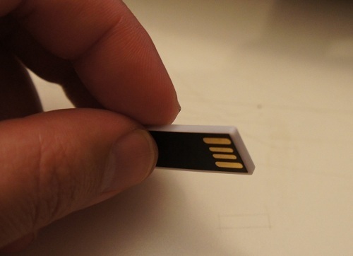
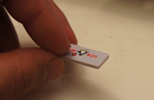
Where USB Memory Sticks are Born
In January, I had the fortune of being a keynote speaker at LCA2013. One of the tchotchkes I received from the conference organizers was a little USB memory stick.
I thought it was a neat coincidence that I was in a factory that manufactured exactly such memory sticks about a week before the conference. In fact, I managed to score a rare treat: the factory owner gave me a sheet of raw chip-on-flex, prior to bonding and encapsulation, to take home.
The USB sticks start life as bare FLASH memory chips. Prior to mounting on PCBs, the chips are screened for capacity and functionality. Below is a photo of the workstation where this happens:
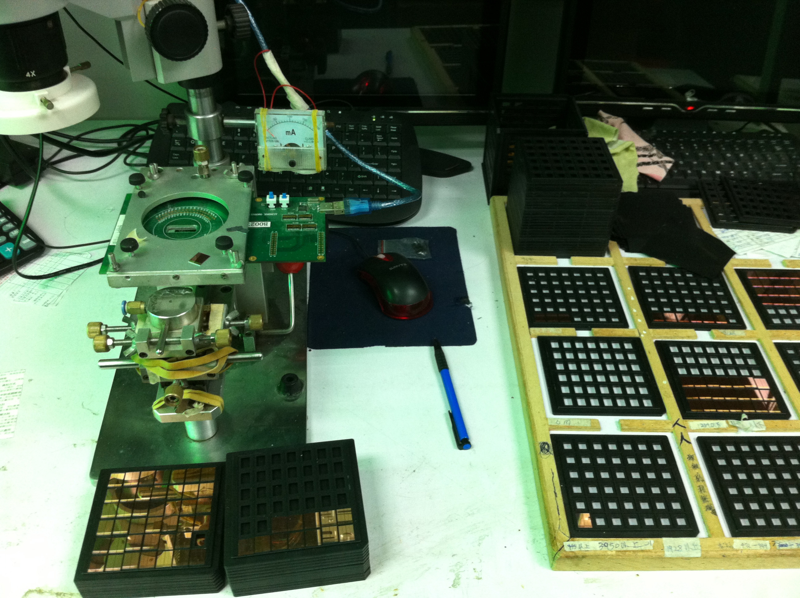
In the image, you can see stacks of bare-die FLASH chips, awaiting screening with a probe card. I love the analog current meter and the use of rubber bands to hold it all together. The probe card has tiny needles on it that touch down on microscopic (less than 100-micron square) contacts on the chip surfaces. Below is what a probe card looks like.
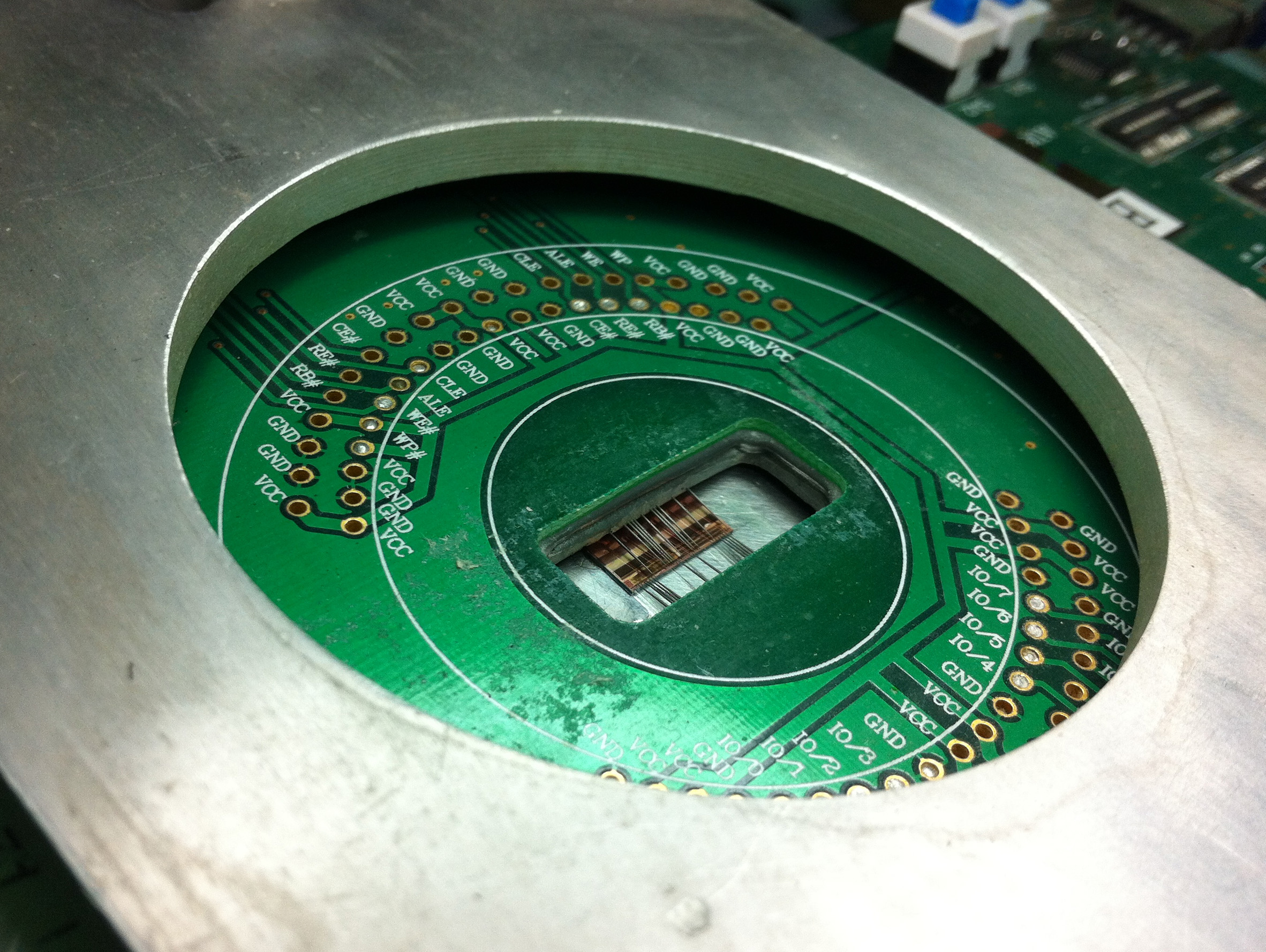
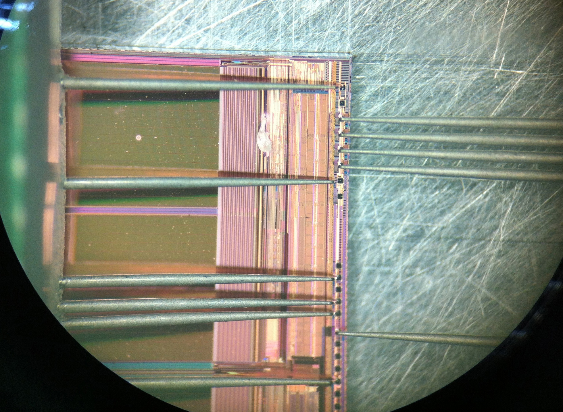
Below is an image through the microscope on the micro-probing station, showing the needles touching down on the square pads at the edge of the FLASH chip’s surface.
Interestingly, this all happens in an absolutely non-clean-room environment. Workers are pretty much handling chips with tweezers and hand suction vises, and mounting the devices into these jigs by hand.
Once the chips are screened for functionality, they are placed by hand onto a PCB. This is not an unusual practice, pretty much every value-oriented wirebonding facility I’ve visited relies on the manual placement of bare die. The photo below shows a controller IC being placed on a panel of PCBs. The bare die are in the right hand side of the photo, sitting in the beige colored waffle pack.
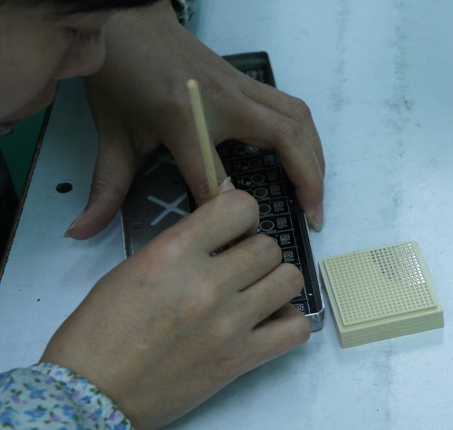
The lady is using some sort of tool made out of hand-cut bamboo. I still haven’t figured out exactly how they work, but every time I’ve seen this process they are using what looks like a modified chopstick to place the chips on the board. My best guess is that the bamboo sticks have just the right surface energy to adhere to the silicon die, such that silicon will stick to the tip of the bamboo rod. A dot of glue is pre-applied to the bare boards, so when the operator touches the die down onto the glue, the surface tension of the glue pulls the die off of the bamboo stick.
It’s trippy to think that the chips inside my USB stick were handled using modified chopsticks.

The chips are then wirebonded to the board using an automated bonding machine which uses image recognition to find the location of the bond pads (this is part of the reason they can get away with manual die placement).
The first half of the video above starts out with the operator pulling off and replacing a mis-bonded wire by hand, and re-feeding the wire into the machine. Given that these wires are thinner than a strand of hair, and that the bonding pads are microscopic, this is no mean feat of manual dexterity.
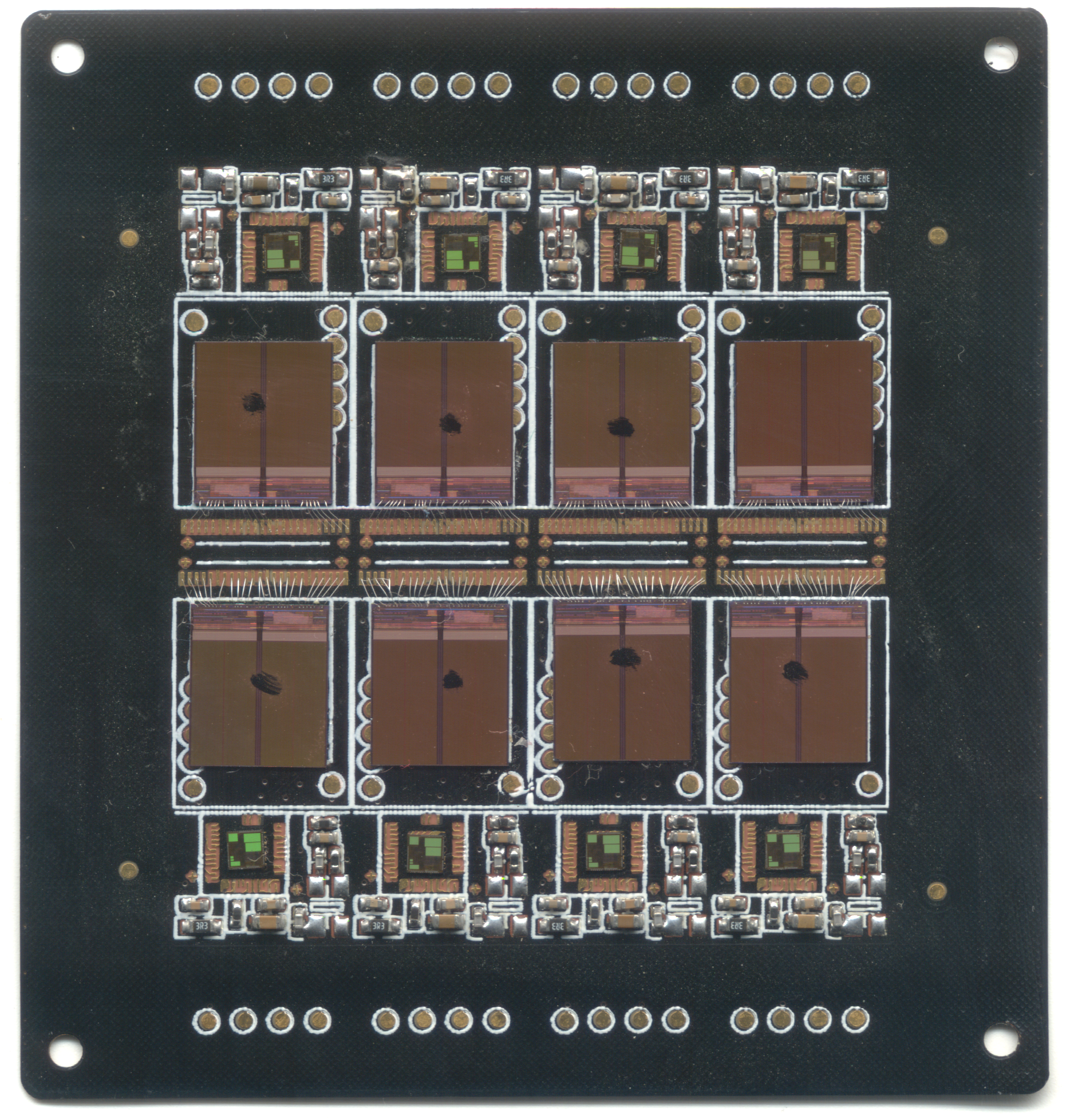
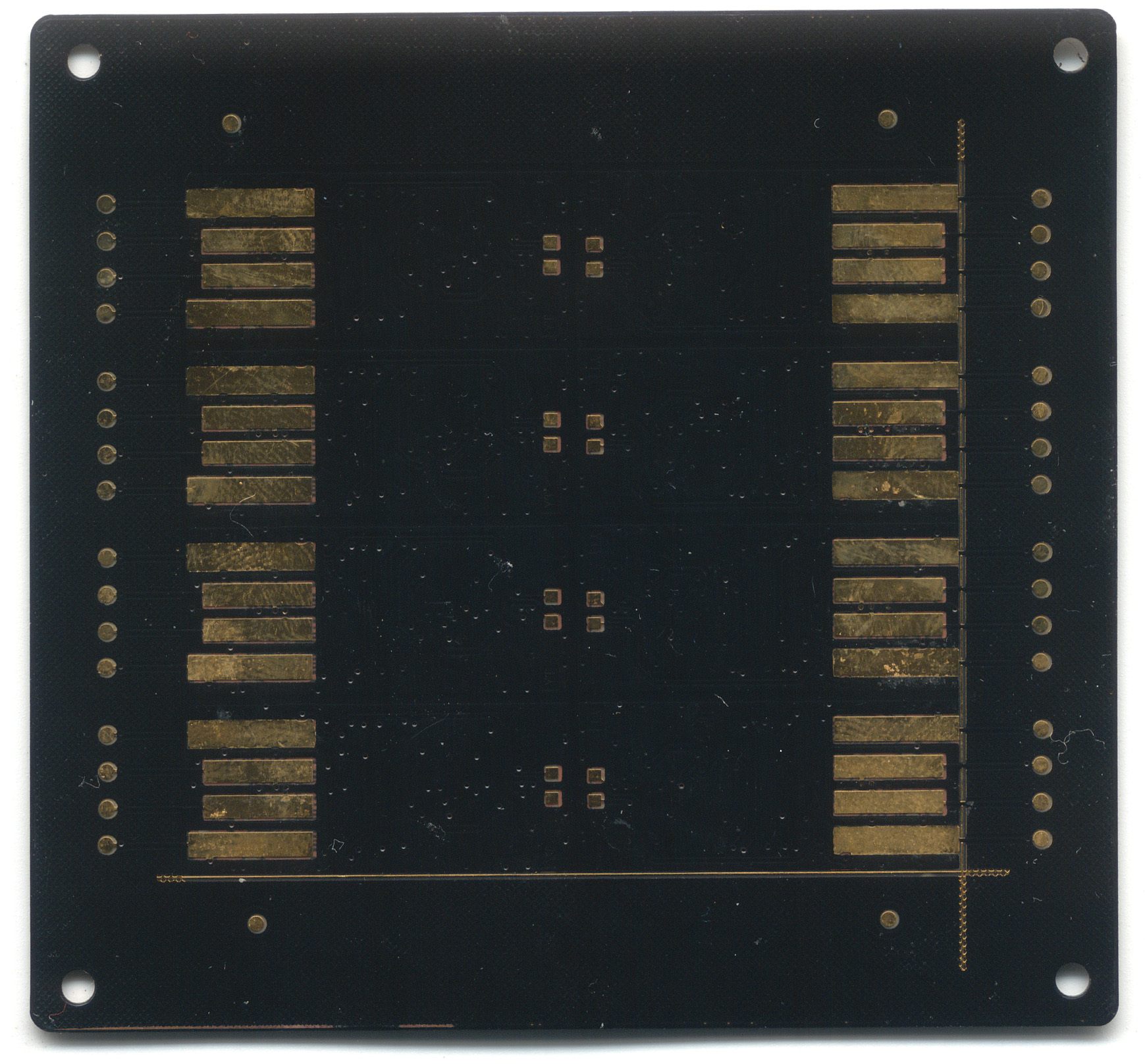
Here’s a scan of the partially-bonded but fully die-mounted PCB that I was given as a memoir from my visit (I had since crushed some of the wire bonds). The panel contains eight USB sticks, each consisting of a FLASH memory chip and a controller IC that handles the bridging between USB and raw FLASH, a non-trivial task that includes managing bad block maps and error-correction, among other things. The controller is probably an 8051-class CPU running at a few dozen MHz.
Once the panels are bonded and tested, they are overmolded with epoxy, and then cut into individual pieces, ready for sale.
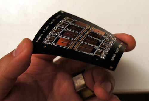
Interestingly, the entire assembly prior to encapsulation is flexible. The silicon chips have been thinned down by grinding off their back sides to the point where they can tolerate a small amount of flexing, and the PCB is also so thin, it is flexible.
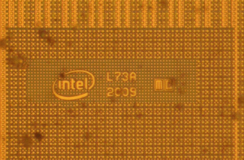
For those of you interested in this kind of thing, here’s the die marking from the FLASH chip; apparently it is made by Intel:
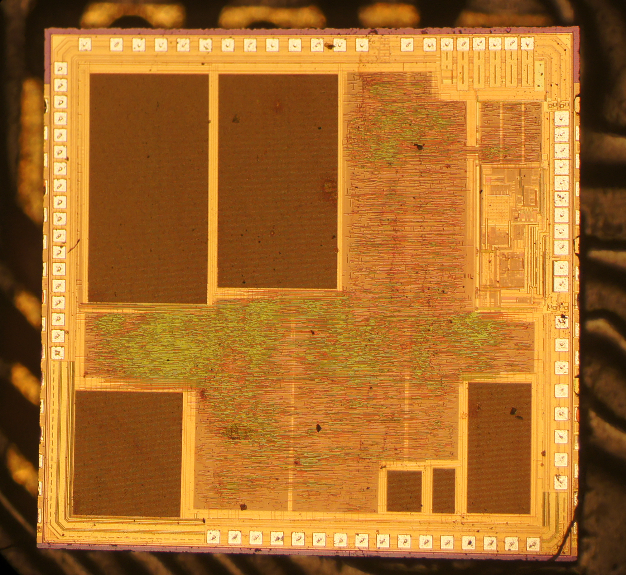
Here is also a die shot of the controller chip:
And now you know where those tiny USB thumb drives are born.
Thanks to David Cranor for contributing images. Images used with permission.
PS: chopsticks
Andrew Huang's Blog

- Andrew Huang's profile
- 32 followers

