
Andrew Huang's Blog, page 39
February 9, 2014
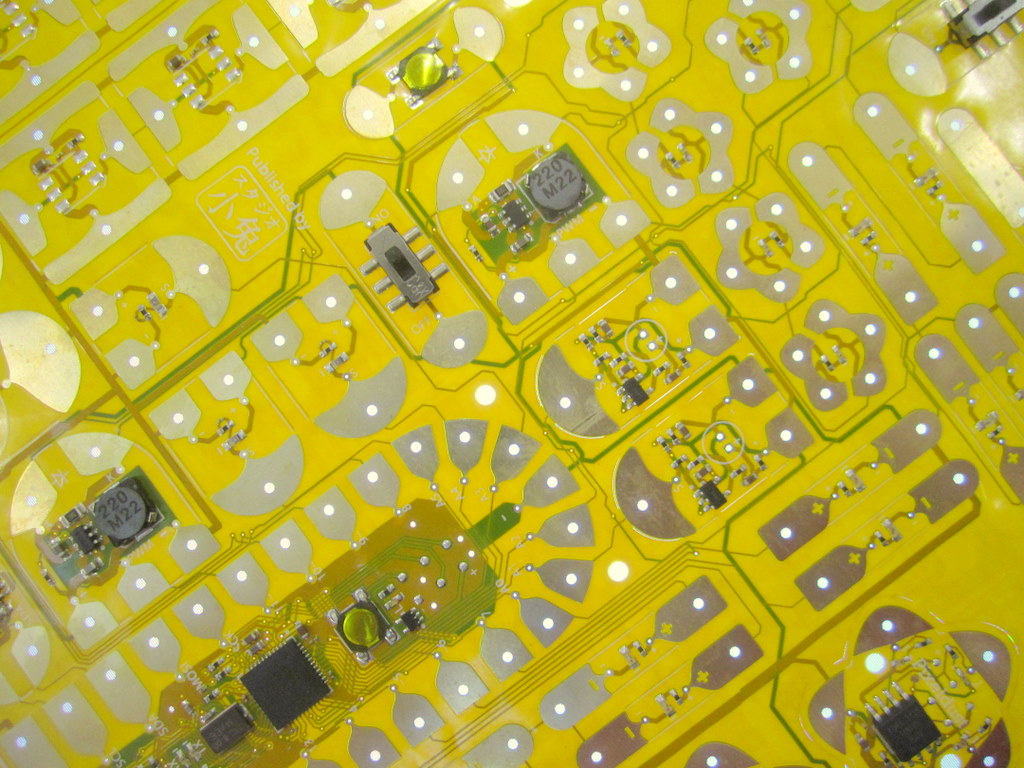
Name that Ware February 2014
The Ware for February 2014 is shown below.
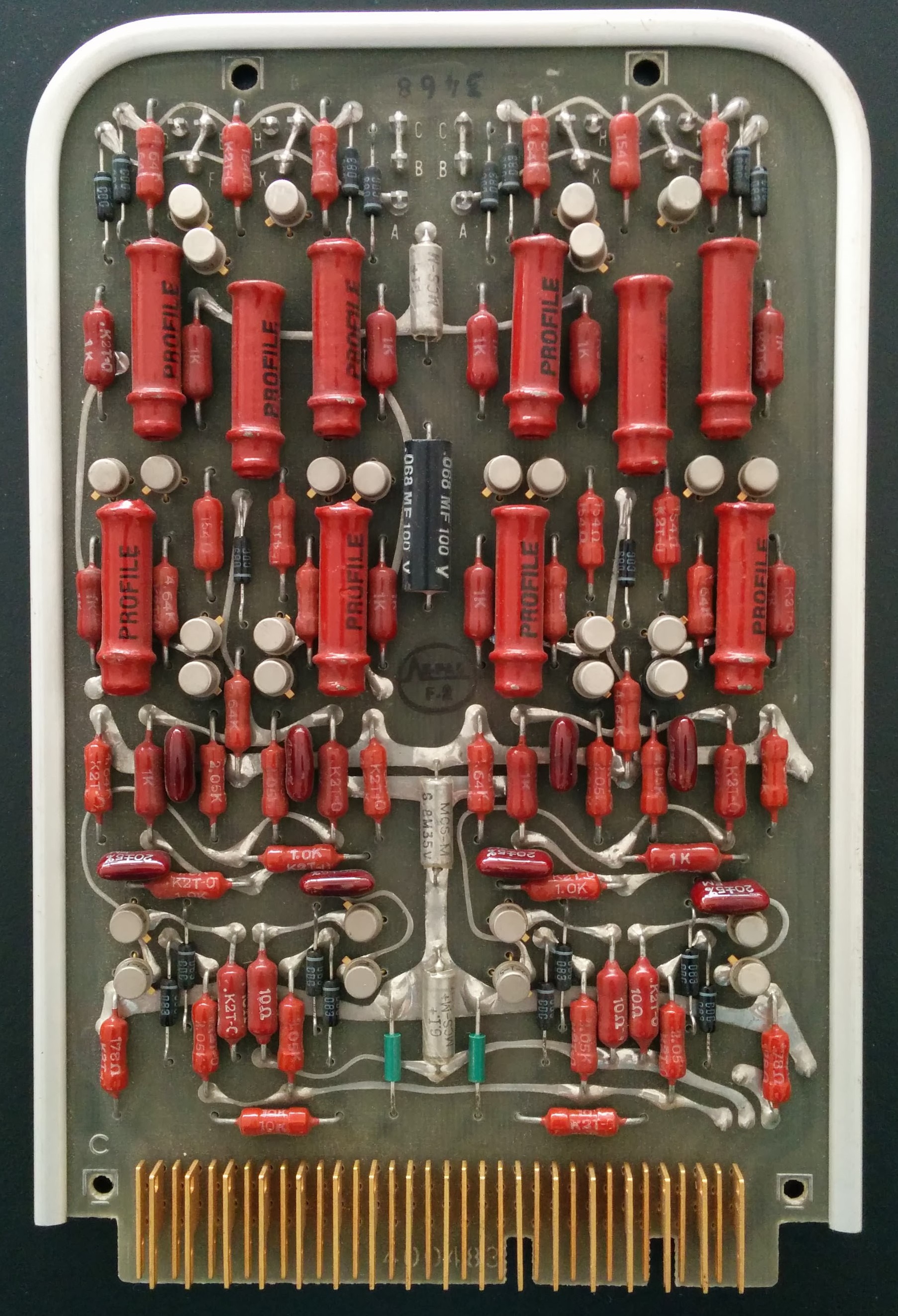
This month’s ware is a handsome bit of retro-computing contributed by Edouard Lafargue (ed _at_ aerodynes.org). The ware was a gift to him from his father.


Winner, Name that Ware January 2014
The Ware for January 2014 was a Chipcom ORnet fiber optic transceiver. Per guessed the ware correctly, and is thus the winner. Congrats, email me for your prize! And thanks again to Mike Fitzmorris for the contribution.
January 8, 2014
Make: Article on Novena
Recently, the Make: blog ran an article on our laptop project, Novena. You can now follow for updates on the project. I’d also like to reiterate here that the photos shown in the article are just an early prototype, and the final forms of the machine are going to be different — quite different — from what’s shown.
Below is a copy of the article text for your convenient reading. And, as a reminder, specs and source files can be downloaded at our wiki.
Building an Open Source Laptop

About a year and a half ago, I engaged on an admittedly quixotic project to build my own laptop. By I, I mean we, namely Sean “xobs” Cross and me, bunnie. Building your own laptop makes about as much sense as retrofitting a Honda Civic with a 1000hp motor, but the lack of practicality never stopped the latter activity, nor ours.
My primary goal in building a laptop was to build something I would use every day. I had previously spent several years at chumby building hardware platforms that I’m ashamed to admit I rarely used. My parents and siblings loved those little boxes, but they weren’t powerful enough for a geek like me. I try to allocate my discretionary funds towards things based on how often I use them. Hence, I have a nice bed, as I spend a third of my life in it. The other two thirds of my life is spent tapping at a laptop (I refuse to downgrade to a phone or tablet as my primary platform), and so when picking a thing to build that I can use every day, a laptop is a good candidate.
 I’m always behind a keyboard!
The project was also motivated by my desire to learn all things hardware. Before this project, I had never designed with Gigabit Ethernet (RGMII), SATA, PCI-express, DDR3, gas gauges, eDP, or even a power converter capable of handling 35 watts – my typical power envelope is under 10 watts, so I was always able to get away with converters that had integrated switches. Building my own laptop would be a great way for me to stretch my legs a bit without the cost and schedule constraints normally associated with commercial projects.
The final bit of motivation is my passion for Open hardware. I’m a big fan of opening up the blueprints for the hardware you run – if you can’t Hack it, you don’t Own it.
Back when I started the project, it was me and a few hard core Open ecosystem enthusiasts pushing this point, but Edward Snowden changed the world with revelations that the NSA has in fact taken advantage of the black-box nature of the closed hardware ecosystem to implement spying measures (“good news, we weren’t crazy paranoids after all”).
Our Novena Project is of course still vulnerable to techniques such as silicon poisoning, but at least it pushes openness and disclosure down a layer, which is tangible progress in the right direction.
While these heady principles are great for motivating the journey, actual execution needs a set of focused requirements. And so, the above principles boiled down to the following requirements for the design:
All the components should have a reasonably complete set of NDA-free documentation. This single requirement alone culled many choices. For example, Freescale is the only SoC vendor in this performance class where you can simply go to their website, click a link, and download a mostly complete 6,000-page programming manual. It’s a ballsy move on their part and I commend them for the effort.
Low cost is not an objective. I’m not looking to build a crippled platform based on some entry-level single-core SoC just so I can compete price-wise with the likes of Broadcom’s non-profit Raspberry Pi platform.
On the other hand, I can’t spec in unicorn hair, although I come close to that by making the outer case from genuine leather (I love that my laptop smells of leather when it runs). All the chips are ideally available off the shelf from distributors like Digi-Key and have at least a five year production lifetime.
Batteries are based off of cheap and commonly available packs used in RC hobby circles, enabling users to make the choice between battery pack size, runtime, and mass. This makes answering the question of “what’s the battery life” a bit hard to answer – it’s really up to you – although one planned scenario is the trans-Siberian railroad trek, which is a week-long trip with no power outlets.
The display should also be user-configurable. The US supply chain is weak when it comes to raw high-end LCD panels, and also to address the aforementioned trans-Siberian scenario, we’d need the ability to drive a low-power display like a Pixel Qi, but not make it a permanent choice. So, I designed the main board to work with a cheap LCD adapter board for maximum flexibility.
No binary blobs should be required to boot and operate the system for the scenarios I care about. This one is a bit tricky, as it heavily limits the wifi card selection, I don’t use the GPU, and I rely on software-only decoders for video. But overall, the bet paid off; the laptop is still very usable in a binary-blob free state. We prepared and gave a talk recently at 30C3 using only the laptops.
The physical design should be accessible – no need to remove a dozen screws just to pull off the keyboard. This design requires removing just two screws.
The design doesn’t have to be particularly thin or light; I’d be happy if it was on par with the 3cm-thick Thinkpads or Inspirons I would use back in the mid 2000′s.
The machine must be useful as a hardware hacking platform. This drives the rather unique inclusion of an FPGA into the mainboard.
The machine must be useful as a security hacking platform. This drives the other unusual inclusion of two Ethernet interfaces, a USB OTG port, and the addition of 256 MiB DDR3 RAM and a high-speed expansion connector off of the FPGA.
The machine must be able to build its own firmware from source. This drives certain minimum performance specs and mandates the inclusion of a SATA interface for running off of an SSD.
After over a year and a half of hard work, I’m happy to say our machines are in a usable form. The motherboards are very reliable, the display is a 13” 2560×1700 (239ppi) LED-backlit panel, and the cases have an endoskeleton made of 5052 and 7075 aluminum alloys, an exterior wrapping of genuine leather, an interior laminate of paper (I also love books and papercraft), and cosmetic panels 3D printed on a Form 1. The design is no Thinkpad Carbon X1, but they’ve held together through a couple of rough international trips, and we use our machines almost every day.
 Laptop parked in front of the Form1 3D printer used to make its body panels.
I was surprised to find the laptop was well-received by hackers, given its homebrew appearance, relatively meager specs and high price. The positive response has encouraged us to plan a crowd funding campaign around a substantially simplified (think “all in one PC” with a battery) case design. We think it may be reasonable to kick off the campaign shortly after Chinese New Year, maybe late February or March. Follow for updates on our progress!

The first two prototypes are wrapped in red sheepskin leather, and green pig suede leather.

Detail view of the business half of the laptop.
January 7, 2014
Name that Ware January 2014
The ware for January is shown below.
Thanks to my buddy Mike Fitzmorris for contributing yet another wonderful ware to this competition.
Winner, Name that Ware December 2013
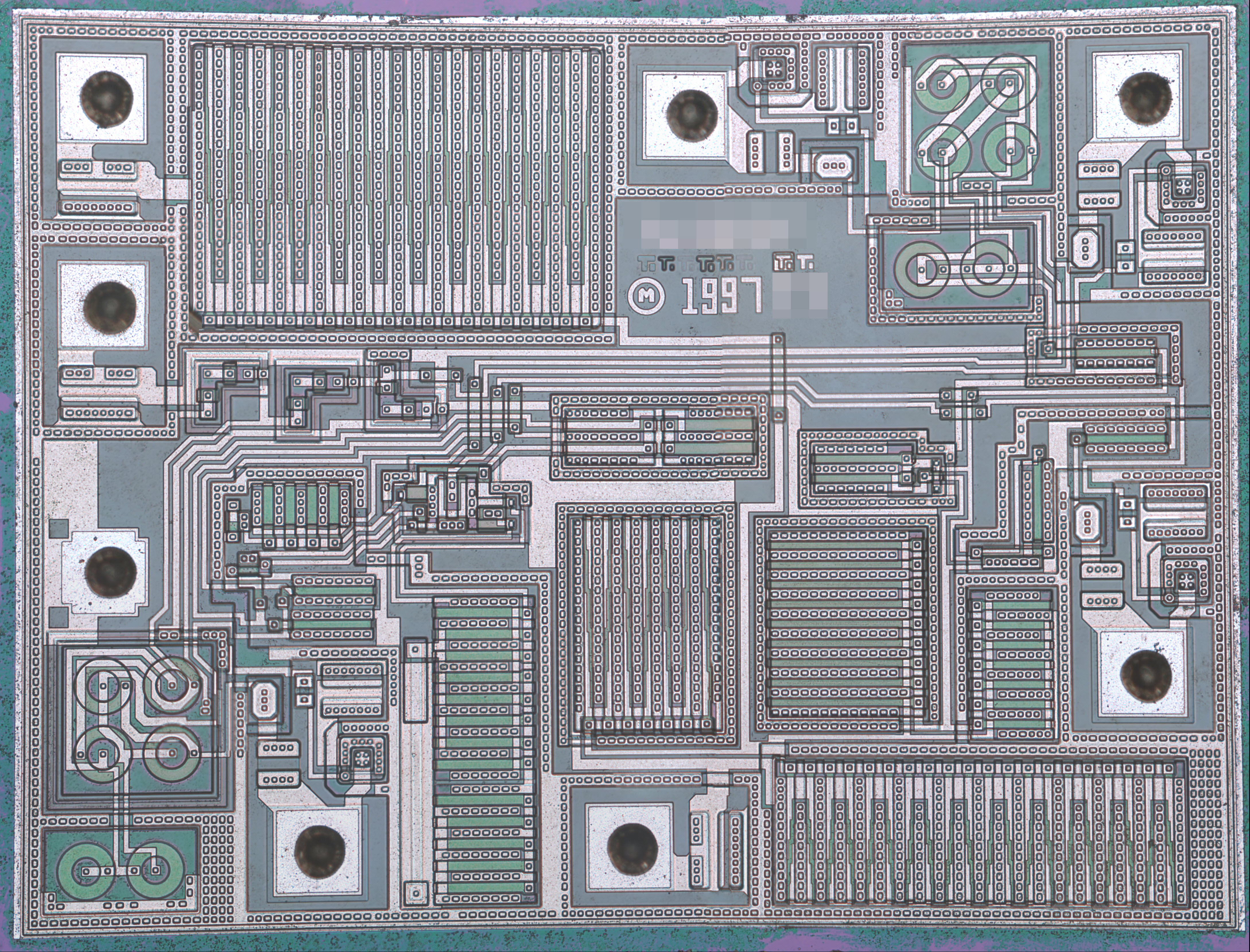
The Ware for last December 2013 is the beloved 555 timer, specifically the TLC555 by TI, fabricated in their “LinCMOS” process. I was very excited when T. Holman allowed me to post this as a ware, partially because I love die shots, and partially because the 555 is such a noteworthy chip and up until now I had never seen the inside of one.
The huge transistor on the top left is the discharge N-FET, and the distinctive, round FETs are I believe what makes LinCMOS special. These are tailor-designed transistors for good matching across process conditions, and they form the front ends of the two differential comparators that are the backbone of the threshold/trigger circuit inside the 555.
Picking a winner this time was tough — many close guesses. I’m going to name “eric” the winner, as he not only properly identified the chip, but also gave extensive analysis in his answer as well. DavidG had a correct guess very early on, but no explanation. Jonathan had the right answer, but the divider underneath the big transistor wasn’t done with resistors, it’s done with FETs, and steveM2 also was very, very close but called it a TLC551Y. So congrats to eric, email me to claim your prize.
December 29, 2013
On Hacking MicroSD Cards
Today at the Chaos Computer Congress (30C3), xobs and I disclosed a finding that some SD cards contain vulnerabilities that allow arbitrary code execution — on the memory card itself. On the dark side, code execution on the memory card enables a class of MITM (man-in-the-middle) attacks, where the card seems to be behaving one way, but in fact it does something else. On the light side, it also enables the possibility for hardware enthusiasts to gain access to a very cheap and ubiquitous source of microcontrollers.
In order to explain the hack, it’s necessary to understand the structure of an SD card. The information here applies to the whole family of “managed flash” devices, including microSD, SD, MMC as well as the eMMC and iNAND devices typically soldered onto the mainboards of smartphones and used to store the OS and other private user data. We also note that similar classes of vulnerabilities exist in related devices, such as USB flash drives and SSDs.
Flash memory is really cheap. So cheap, in fact, that it’s too good to be true. In reality, all flash memory is riddled with defects — without exception. The illusion of a contiguous, reliable storage media is crafted through sophisticated error correction and bad block management functions. This is the result of a constant arms race between the engineers and mother nature; with every fabrication process shrink, memory becomes cheaper but more unreliable. Likewise, with every generation, the engineers come up with more sophisticated and complicated algorithms to compensate for mother nature’s propensity for entropy and randomness at the atomic scale.
These algorithms are too complicated and too device-specific to be run at the application or OS level, and so it turns out that every flash memory disk ships with a reasonably powerful microcontroller to run a custom set of disk abstraction algorithms. Even the diminutive microSD card contains not one, but at least two chips — a controller, and at least one flash chip (high density cards will stack multiple flash die). You can see some die shots of the inside of microSD cards at a microSD teardown I did a couple years ago.
In our experience, the quality of the flash chip(s) integrated into memory cards varies widely. It can be anything from high-grade factory-new silicon to material with over 80% bad sectors. Those concerned about e-waste may (or may not) be pleased to know that it’s also common for vendors to use recycled flash chips salvaged from discarded parts. Larger vendors will tend to offer more consistent quality, but even the largest players staunchly reserve the right to mix and match flash chips with different controllers, yet sell the assembly as the same part number — a nightmare if you’re dealing with implementation-specific bugs.
The embedded microcontroller is typically a heavily modified 8051 or ARM CPU. In modern implementations, the microcontroller will approach 100 MHz performance levels, and also have several hardware accelerators on-die. Amazingly, the cost of adding these controllers to the device is probably on the order of $0.15-$0.30, particularly for companies that can fab both the flash memory and the controllers within the same business unit. It’s probably cheaper to add these microcontrollers than to thoroughly test and characterize each flash memory chip, which explains why managed flash devices can be cheaper per bit than raw flash chips, despite the inclusion of a microcontroller.
The downside of all this complexity is that there can be bugs in the hardware abstraction layer, especially since every flash implementation has unique algorithmic requirements, leading to an explosion in the number of hardware abstraction layers that a microcontroller has to potentially handle. The inevitable firmware bugs are now a reality of the flash memory business, and as a result it’s not feasible, particularly for third party controllers, to indelibly burn a static body of code into on-chip ROM.
The crux is that a firmware loading and update mechanism is virtually mandatory, especially for third-party controllers. End users are rarely exposed to this process, since it all happens in the factory, but this doesn’t make the mechanism any less real. In my explorations of the electronics markets in China, I’ve seen shop keepers burning firmware on cards that “expand” the capacity of the card — in other words, they load a firmware that reports the capacity of a card is much larger than the actual available storage. The fact that this is possible at the point of sale means that most likely, the update mechanism is not secured.
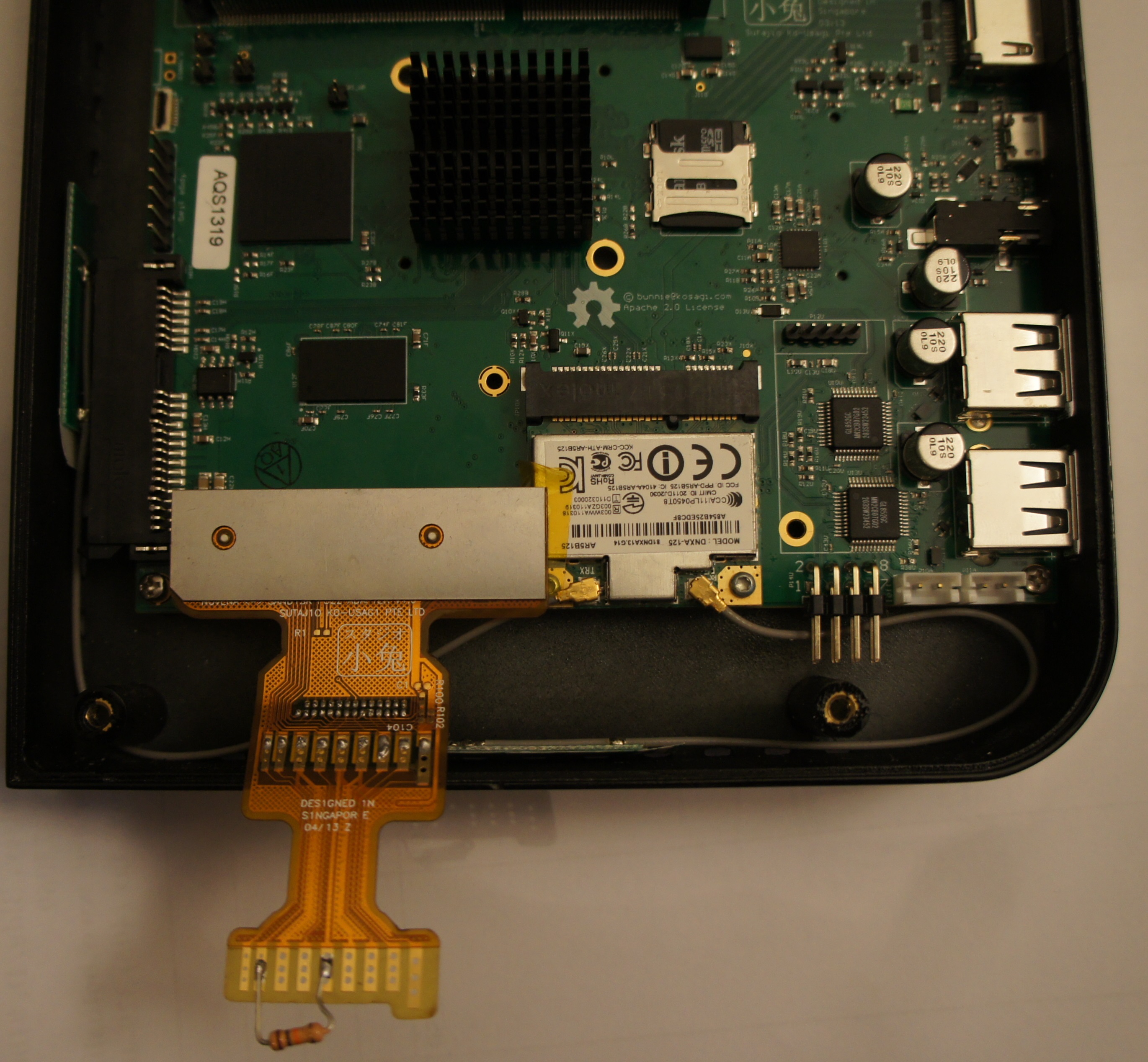
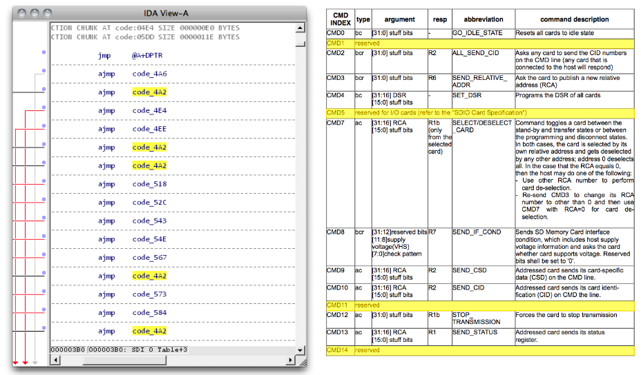
In our talk at 30C3, we report our findings exploring a particular microcontroller brand, namely, Appotech and its AX211 and AX215 offerings. We discover a simple “knock” sequence transmitted over manufacturer-reserved commands (namely, CMD63 followed by ‘A’,'P’,'P’,'O’) that drop the controller into a firmware loading mode. At this point, the card will accept the next 512 bytes and run it as code.
From this beachhead, we were able to reverse engineer (via a combination of code analysis and fuzzing) most of the 8051′s function specific registers, enabling us to develop novel applications for the controller, without any access to the manufacturer’s proprietary documentation. Most of this work was done using our open source hardware platform, Novena, and a set of custom flex circuit adapter cards (which, tangentially, lead toward the development of flexible circuit stickers aka chibitronics).
Significantly, the SD command processing is done via a set of interrupt-driven call backs processed by the microcontroller. These callbacks are an ideal location to implement an MITM attack.
It’s as of yet unclear how many other manufacturers leave their firmware updating sequences unsecured. Appotech is a relatively minor player in the SD controller world; there’s a handful of companies that you’ve probably never heard of that produce SD controllers, including Alcor Micro, Skymedi, Phison, SMI, and of course Sandisk and Samsung. Each of them would have different mechanisms and methods for loading and updating their firmwares. However, it’s been previously noted that at least one Samsung eMMC implementation using an ARM instruction set had a bug which required a firmware updater to be pushed to Android devices, indicating yet another potentially promising venue for further discovery.
From the security perspective, our findings indicate that even though memory cards look inert, they run a body of code that can be modified to perform a class of MITM attacks that could be difficult to detect; there is no standard protocol or method to inspect and attest to the contents of the code running on the memory card’s microcontroller. Those in high-risk, high-sensitivity situations should assume that a “secure-erase” of a card is insufficient to guarantee the complete erasure of sensitive data. Therefore, it’s recommended to dispose of memory cards through total physical destruction (e.g., grind it up with a mortar and pestle).
From the DIY and hacker perspective, our findings indicate a potentially interesting source of cheap and powerful microcontrollers for use in simple projects. An Arduino, with its 8-bit 16 MHz microcontroller, will set you back around $20. A microSD card with several gigabytes of memory and a microcontroller with several times the performance could be purchased for a fraction of the price. While SD cards are admittedly I/O-limited, some clever hacking of the microcontroller in an SD card could make for a very economical and compact data logging solution for I2C or SPI-based sensors.
Slides from our talk at 30C3 can be downloaded here, or you can watch the talk on Youtube below.
Team Kosagi would like to extend a special thanks to .mudge for enabling this research through the Cyber Fast Track program.
December 9, 2013
Name that Ware December 2013
The Ware for December 2013 is shown below.
It’s been a while since I’ve had a proper die shot for a name that ware. Thanks to T. Holman for sharing this ware with us!
Winner, Name that Ware November 2013
The Ware for November 2013 is anisotropic conductive tape, aka “Z-tape”. When I first heard about Z-tape, I scratched my head and wondered how that could work; but after lighting it up under a microscope, I instantly had a clear intuition for how it works, and its limitations.
The winner for last month’s competition is Scott Roberts, who for the record entered the correct guess prior to the answer being posted a couple days later in a follow-up post about circuit stickers. Congrats, email me for your prize!
November 28, 2013
haxlr8r Map of Shenzhen Electronics Market
I’m fond of trawling the electronic markets of Shenzhen. It’s a huge area, several city blocks; it is overwhelming in scale. My friends at haxlr8r have published a guide to the markets, targeted at helping intrepid hacker-engineers use the market more efficiently, without having to spend a couple of weeks just figuring out the basics.
This is the first guide I’ve seen that gives a floor-by-floor breakdown of the wares contained in each building. This is particularly handy as some buildings contain several specialties that are not reflected by the items you find on the ground floor. It’s also bi-lingual, which helps if you can’t speak the language and you need to point at something the locals can read. While the map is missing a couple of my favorite spots, overall it’s well done and took a lot of effort to compile.
If you’re into making electronics, this electronics market is a must-see destination. If you have an idea you’re itching to build, you might want to consider applying to haxlr8r (currently accepting applications until November 30th). haxlr8r’s offices are right in the heart of the electronics district, and I’m a mentor for the program; so, it’s a great opportunity to learn the markets, build stuff, and hang out and have a few beers.
November 18, 2013
Introducing chibitronics
Today, my collaborator Jie Qi and I launched a Crowd Supply campaign for circuit stickers.
Please visit the campaign page to see more photos of the stickers and to see how they can be used.
Here, I will write a bit about the background story, tech details, and manufacturing processes that went into making them.
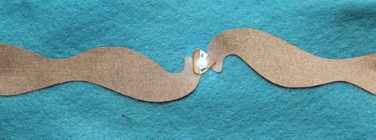
Circuit stickers are peel-and-stick electronics for crafting circuits. In a nutshell, they are circuits on a flexible polyimide substrate with anisotropic tape (or “Z-tape” — so named because electricity only flows vertically through the tape, and not laterally) laminated on the back.
The use of Z-tape allows one to assemble circuits without the need for high-temperature processing (e.g. soldering or reflow), thereby enabling compatibility with heat-sensitive and/or pliable material substrates, such as paper, fabric, plastic, and so forth.
This enables electronics to be integrated in a range of non-traditional material systems with great aesthetic effect, as exemplified by the addition of circuit stickers to fabric and paper, shown below.

The Backstory
In today’s world of contract manufacturing and turnkey service providers, designers tend to pick from a palette of existing processes to develop products. Most consumer electronic devices are an amalgamation of rigid PCB, reflow/wave soldering, ABS/PC injection molding, sheet metal forming, and some finishing processes such as painting or electroplating. This palette is sufficient to cover the full range of utility required by most products, but I’ve noticed that really outstanding products also tend to introduce new materials or novel manufacturing processes.
I’ve a long-running hypothesis that new process development doesn’t have to be expensive, as long as you yourself are willing to go onto the factory floor and direct the improvements. In other words, the expensive bit is the wages of the experts developing the process, not the equipment or the materials.
I decided to start exploring flex circuits as a design medium, under the reasoning that although flex circuit technology is common place inside consumer products — there’s probably a half dozen examples of flex PCB inside your mobile phone — it’s underrepresented in hobby & DIY products. I had a hunch that the right kind of product designed in flex could enable new and creative applications, but I wasn’t quite sure how. One of my “training exercises” was a flex adapter for emulating a TSOP NAND FLASH chip, which I had written about previously on this blog.
The moment of serendipity came last January, when I was giving a group of MIT Media Lab students a tour of Shenzhen. Jie Qi, a PhD candidate at the Media Lab, showed me examples of her work combining electronics and papercraft.
Clearly, circuits on flex could be an interesting addition to this new media, but how? Building circuits on flex and then soldering the flex circuit onto paper would be an improvement, but it’s only an incremental improvement. We wanted a solution that would be compatible with low-melting point materials; furthermore, being solder-free meant that the stickers could be used in contexts where using a soldering iron is impractical or prohibited.
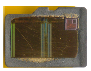
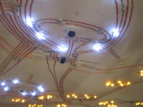
Jie introduced me to Z-tape, which is a great solution to the problem. November’s ware is a 20x magnification of Z-tape laminated to the back of a circuit sticker (someone has, of course, already correctly guessed the ware at the time of writing, so I can discuss the ware in more detail here without ruining the contest).

The stipples in the photo above (click on it for a larger version) are tiny metal particles that span from one side of the adhesive layer to the other. As you can see, the distribution is statistical in nature; therefore, in order to ensure good contact, a large pad area is needed. Furthermore, traces very close to each other can be shorted out by the embedded metal particles, so as I design the circuits I have to be careful to make sure I have enough space between exposed pads. The datasheet for the Z-tape material contains rules for the minimum pad size and spacing.
The problem is that there were no standard manufacturing processes that could produce circuit stickers as we envisioned them. Here at last was a meaningful opportunity to test the theory that new process development can be done on the cheap, as long as you are willing to do it yourself. And so, I started my own little research program to explore flexible circuit media, and the challenges of making circuit stickers out of them, all on Studio Kosagi’s shoe string R&D budget.
The first thing I did was to visit the facility where flex PCBs are manufactured. The visit was eye-opening.
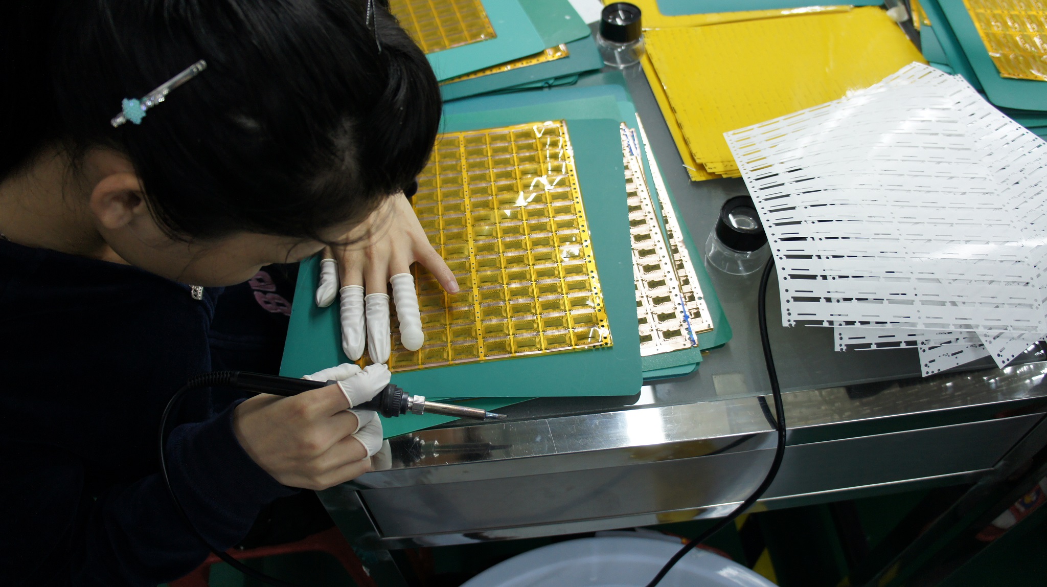
Above is a worker manually aligning coverlay onto flex circuit material. Coverlay is a polyimide sheet used instead of soldermask on flex circuits. Soldermask is too brittle, and will crack; therefore, for reliability over thousands of flexing cycles, a coverlay is recommended.
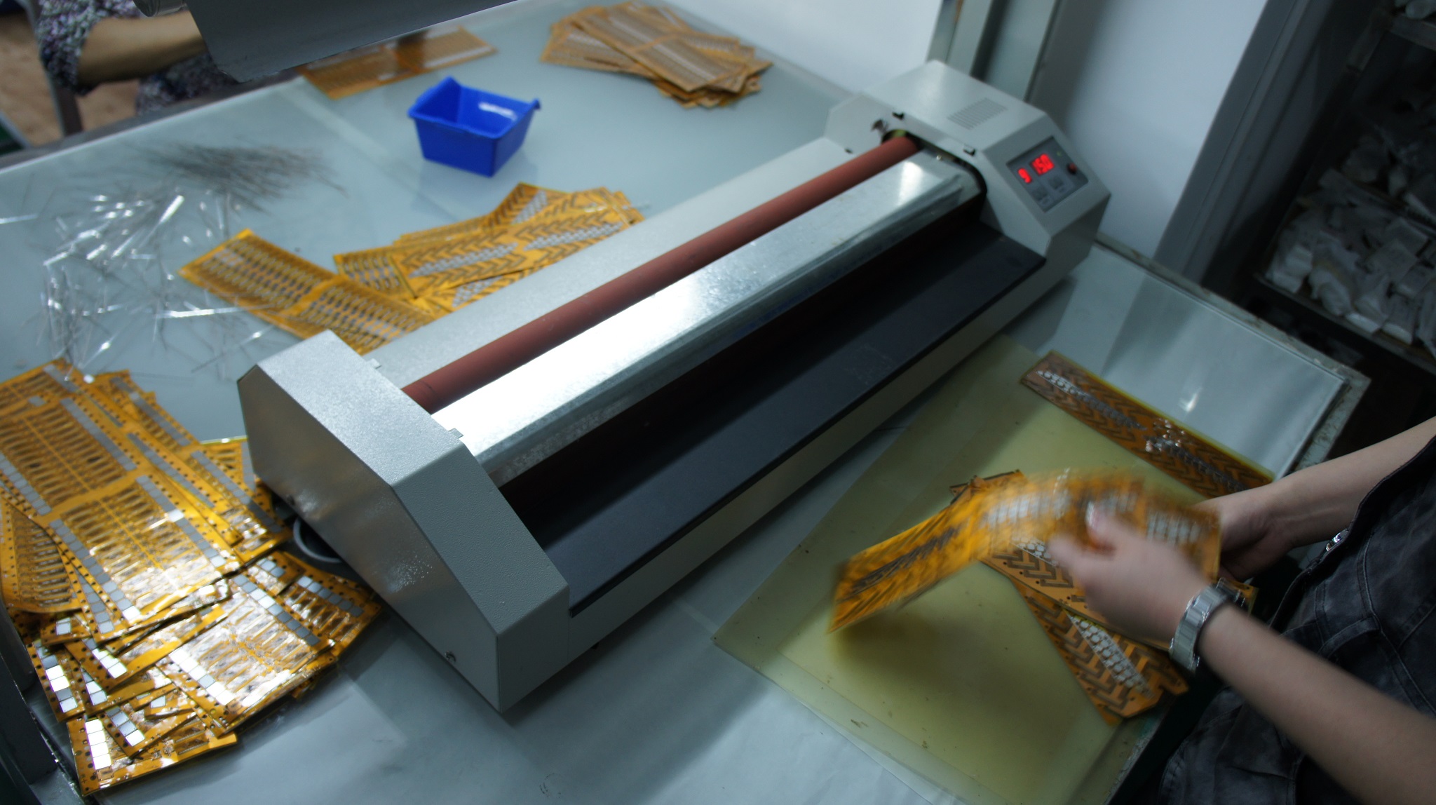
Above is an example of steel plates being laminated to the back of flex circuit material. In some situations, it’s desirable for portions of the flex circuit to be stiff: either for mechanical mounting, or to help with SMT processing. I knew that it was possible to laminate polyimide stiffiners to flex, but I didn’t know that steel lamination was also possible until I took the factory tour.
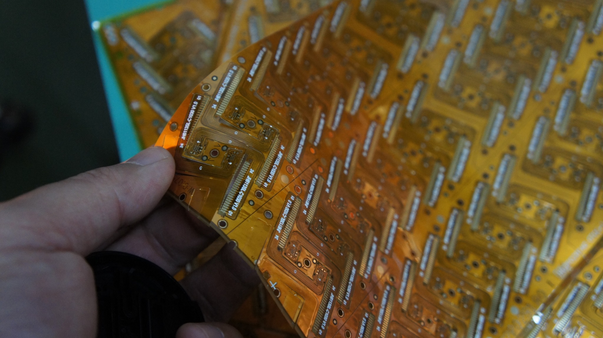
Above is an example of the intricate shapes achievable with die cutting.
After visiting the factory, we decided the next step was to do a process capability test. The purpose of this test is to push the limits of the manufacturing process — intentionally breaking things to discover the weak links. Our design exercised all kinds of capabilities — long via chains, 3-mil line widths, 0201 components, 0.5mm pitch QFN, bulky components, the use of soldermask instead of coverlay, fine detail in silkscreening, captive tabs, curved cut-outs, hybrid SMT and through hole, Z-tape lamination, etc.
Below are some images of what our process capability test design looked like.
When I first presented the design to the factory, it was outright rejected as impossible to manufacture. However, after explaining my goals, they consented to produce it, with the understanding that I would accept and pay for all the units made including the defective units (naturally). Through analyzing the failure modes of the defective units, I was able to develop a set of design rules for maintaining high yield (and therefore lowering cost) on the circuit stickers.
In my next post on chibitronics, I’ll go into how we co-developed the final design and manufacturing process for the stickers. I will also have a post talking about how we developed the partial perforation die cut manufacturing process that enables the convenient peel-and-stick format for the stickers.
I’ll also have a post on why we decided to go with Crowd Supply instead of Kickstarter, and why we picked $1 as a funding goal.
Andrew Huang's Blog

- Andrew Huang's profile
- 32 followers

